
With multiple functionalities added into a single chip, be it a SoC or an ASIC, maintaining low power consumption has become critical for any design. Various techniques at the technology as well as design level are employed to accomplish the low power target. These include thinner oxides in transistors, different sections of the design working at different voltage levels, the design architected into multiple power domains which can then be switched on or off as per need and so on. In order to make smooth transition between different voltages, circuit elements such as level shifters are used. Similarly retention cells are used to keep input state of any switched-off power domain intact. However, such designs with multiple power domains are prone to subtle errors which are easy to commit but very difficult to detect through conventional tools and methodologies such as SPICE simulation or P&R methodologies (because P&R tools mostly work at gate level).

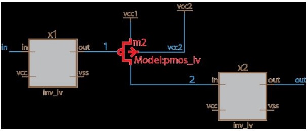
[A transistor connected to difference VCCs – Susceptible to performance degradation]
As an example, in the above figure, a transistor is connected to VCC1 and VCC2 which can be at the same voltage but in different domains, hence switching on and off at different times. This issue may not be detected by usual SPICE simulation. Again, if VCC2 has a higher voltage than VCC1, the gate oxide becomes vulnerable to breakdown. Such issues may not cause immediate failure of the circuit, but can lead to performance degradation and affect reliability in the long run.
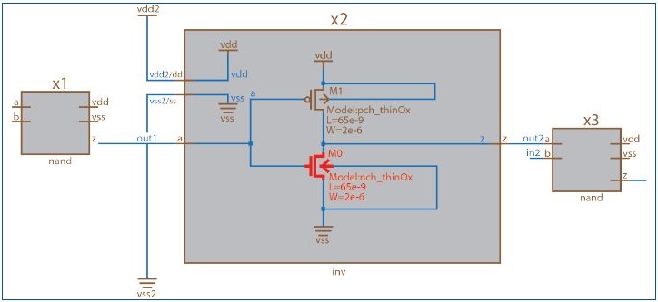
[An IP connected incorrectly to external power terminals]
In case of SoCs containing multiple IPs, it becomes further complicated because the IPs can be at different voltage levels and power domains and need to be hooked up correctly in the larger implementation of semiconductor design. Power domain crossing errors are very prevalent in these cases. In the above figure, although voltages internal to the IP block are consistent, externally it has been hooked up incorrectly. These kinds of issues can render the devices to multiple issues such as changed threshold voltages and switching times, ultimately leading to degradation of the whole chip.
Talking about how to overcome these issues, Calibre PERC from Mentor Graphics provides robust transistor-level power intent verification by leveraging the power intent information annotated in UPF (Unified Power Format) that comes along as an integral part of the whole design flow. Calibre PERC identifies the right voltage combinations and assigns them as per design’s power intent, thus improving verification coverage and robustness
Calibre PERC is able to leverage design flows with or without UPF to understand the power intent down to the transistor level and then apply reliability verification at the transistor level. It ensures correct implementation of low-power rules, use of level shifters and other protection circuitry etc. Calibre PERC also detects all thin oxide transistors in the circuit and takes extra care to catch voltages which can lead to their oxide breakdown.
Users can easily insert reliability verification into their existing design flows with Calibre PERC as part of an integrated Calibre platform for cell, block, and full-chip verification. Those rules can be in standard SVRF and TVF formats, thus maintaining compatibility with designs and foundries.
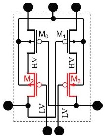
To reduce the debugging complexity, Calibre PERC eliminates false errors by recognizing particular topologies (such as level shifters and isolation cells) used to enable power domain transitions at the right level. In the figure on the right side, Calibre PERC can identify these structures as level shifters and then the errors on M2 and M3 can be waived.
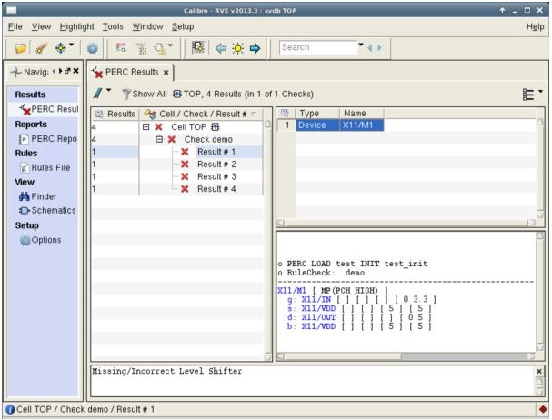
[Calibre RVE – Result viewing and debugging environment]
Calibre RVE is a novel result viewing and debugging environment which makes debugging reliability checks easy, quick and thorough.
I was impressed with the capabilities of Calibre PERC in the power and reliability verification and its easy integration into sign-off flows. A detailed analysis of power related issues and how calibre solves those is given in one of the Mentor’s whitepapers here. Interesting read!!
lang: en_US


Comments
There are no comments yet.
You must register or log in to view/post comments.