You are currently viewing SemiWiki as a guest which gives you limited access to the site. To view blog comments and experience other SemiWiki features you must be a registered member. Registration is fast, simple, and absolutely free so please,
join our community today!
I talked to John Lee (GM of the ANSYS Semiconductor BU) recently about his views on market trends and the ANSYS big-picture theme for DAC 2018. He set the stage by saying he really liked Wally’s view on trends (see my blog on Wally’s keynote at U2U). John said these confirm what he is seeing – a trend to specialization, some around… Read More
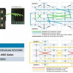
The advantages of prototyping a hardware design on a FPGA platform are widely recognized, for software development, debug and regression in particular while the ultimate ASIC hardware is still in development. And if your design will fit into a single FPGA, this is not an especially challenging task (as long as you know your way … Read More
FPGA Design Gets Realby Tom Simon on 02-08-2017 at 12:00 pmCategories: EDA, FPGA, Synopsys
FPGA’s have become an important part of system design. It’s a far cry from how FPGA’s started out – as glue logic between discrete logic devices in the early days of electronic design. Modern day FPGA’s are practically SOC’s in their own right. Frequently they come with embedded processor cores, sophisticated IO cells, DSP,… Read More
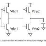
Variation is still the tough nut to crack for advanced process nodes. The familiar refrain of lower operating voltages and higher performance requirements make process variation an extremely important design consideration. As far back as the early 2000’s design teams have been looking for a better approach to model variation… Read More
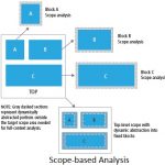
The challenge of tracking design progress is a shared problem for individual designers, team leaders, and project managers. At each level the ability to step back from just reviewing error log files and seeing the arc of the whole design as it moves forward is valuable. The difficulty of seeing the whole picture is exacerbated when… Read More
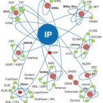
Although I knew about Crossfire’s capabilities for signing off quality of an IP before its integration into an SoC, there was much more to learn about this tool when I visited Fractal Technologies booth during this DAC. The complexity handled by this tool to qualify any type of IP for its integration into an SoC can be imagined by the… Read More
In Chaucer’s Canterbury Tales, the second of the tales told by the pilgrims is The Miller’s Tale. Since this is a family blog, I’ll leave you to research the tale yourself. But FinFETs hide another Miller’s Tale, due to Miller capacitance, sometimes called the Miller effect. This is significant since in FinFET designs Miller capacitance… Read More
With the unprecedented increase in semiconductor design size and complexity design teams are required to accommodate multiple design constraints such as multiple power domains for low power design, multiple modes of operation, many clocks running, and third party IPs with different SDCs. As a result timing closure has become… Read More
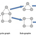
I think by now a lot has been said about the necessity of multi-patterning at advanced technology nodes with extremely low feature size such as 20nm, because lithography using 193nm wavelength of light makes printing and manufacturing of semiconductor design very difficult. The multi-patterning is a novel semiconductor manufacturing… Read More
The semiconductor design sizes, these days, can easily be of the order of several hundred millions of cells, adding into the complexity of verification. Amid ever growing design sizes, it’s a must that the timing verification is done accurately. Normally Static Timing Analysis (STA) is done to check whether all clocks and signals… Read More