You are currently viewing SemiWiki as a guest which gives you limited access to the site. To view blog comments and experience other SemiWiki features you must be a registered member. Registration is fast, simple, and absolutely free so please,
join our community today!
            WP_Term Object
(
    [term_id] => 1561
    [name] => ESD Alliance
    [slug] => esd-alliance
    [term_group] => 0
    [term_taxonomy_id] => 1561
    [taxonomy] => category
    [description] =>
    [parent] => 386
    [count] => 125
    [filter] => raw
    [cat_ID] => 1561
    [category_count] => 125
    [category_description] =>
    [cat_name] => ESD Alliance
    [category_nicename] => esd-alliance
    [category_parent] => 386
    [is_post] =>
)

WP_Term Object
(
    [term_id] => 1561
    [name] => ESD Alliance
    [slug] => esd-alliance
    [term_group] => 0
    [term_taxonomy_id] => 1561
    [taxonomy] => category
    [description] =>
    [parent] => 386
    [count] => 125
    [filter] => raw
    [cat_ID] => 1561
    [category_count] => 125
    [category_description] =>
    [cat_name] => ESD Alliance
    [category_nicename] => esd-alliance
    [category_parent] => 386
    [is_post] =>
)
I will be at Semicon West from 9th to 11th July in Moscone, San Francisco. Of course there are lots of interesting sessions but here are two that I think are especially important to get a good impression of the way things are going in the future from experts. The two most interesting questions about the future are what comes after 14nm,… Read More
They are three of the top trending terms on SemiWiki and three of the hot topics at this year’s Semicon West:
In its 43rd year, SEMICON West is the flagship annual event for the global microelectronics industry. It is the premier event for the display of new products and technologies for microelectronics design and manufacturing,… Read More
So where in the world do you think semiconductor manufacturing is increasing the fastest? OK, Taiwan, that was pretty easy. But in second place, with over 20% of the world’s semiconductor equipment capital investment is the US. Growing faster than Europe, China, Japan and equal with Korea.
This was not the case half a dozen… Read More
I’ve been digging around the Interwebs a bit trying to find out what the received wisdom is about how big a cost reduction can be expected if and when we transition to 450mm (18″) wafers from today’s standard of 300mm (12″). And the answers are totally all over the place. They vary from about a 30% cost reduction… Read More
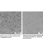
At Semicon, Ben Rathsack of Tokyo Electron America talked about directed self assembly (DSA) at the standing-room only lithography morning. So what is it? Self assembly involves taking two monomers that don’t mix and letting them polymerise (so like styrene forming polystyrene). Since they won’t mix they will … Read More
I attended a panel session followed by a party during Semicon to celebrate Soitec’s 20th birthday. Officially it was titled An Insider’s Look at the Future of Mobile Technologies. But in reality it was a look at the future possibilities for SOI.
Silicon on Insulator (SOI) has been a sort of bastard child of semiconductor.… Read More
One of the presenters at the standing-room only litho session at Semicon this week was Serge Tedesco, the litho program manager at CEA-Leti in Grenoble France. He is running a program called IMAGINE for maskless lithography. Chips today are built using a reticle (containing the pattern for that layer of the chip) which is exposed… Read More
I have been spending some time at Semicon West at the Moscone center the last couple of days. Since it was only a month ago that I was there for DAC, the first contrast is the size of the show. DAC didn’t fill Moscone South. Semicon fills Moscone South, and North, and the corridor between. And Moscone West on the other side of 4th … Read More
Yesterday’s SEMICO IP Ecosystem Conference was well worth the time. Everybody was there: ARM, Synopsys, Cadence, Mentor Graphics, GlobalFoundries, TSMC, MIPS, Tensilica, AMD, Atrenta, Sonics, and Tabula, everybody except Intel of course. What do Intel and I have in common? We don’t play well with others…
First up was… Read More