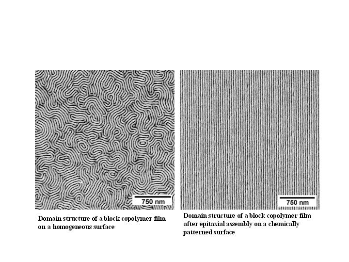

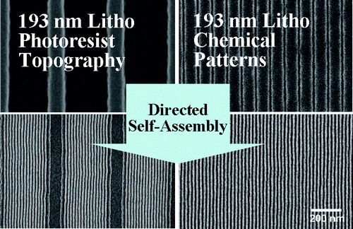
At Semicon, Ben Rathsack of Tokyo Electron America talked about directed self assembly (DSA) at the standing-room only lithography morning. So what is it? Self assembly involves taking two monomers that don’t mix and letting them polymerise (so like styrene forming polystyrene). Since they won’t mix they will form up into separate areas for the two polymers. If you do nothing else you will end up with somewhat random patterns like a fingerprint. But if you provide guides, either physical guides by putting material on the wafer at a coarse density, or chemical guides by putting a thin coat of something that attracts one of the polymers, instead of a random pattern you get a sort of amplification of the pattern you laid down but at much finer grain.

For example, if you put down material at 80nm spacing you can end up with the two polymers lining up and alternating at 28nm.
Holes (for contact/via cuts) are trickier. It is easy enough to get a honeycomb pattern with the two polymers but a grid is harder. But it turns out that by adding a guide in the form of a larger trench, and then putting the polymers into the trench that they self assemble (if in the right ratio) into an outer polymer with a line of holes up the middle.
You can’t get a chip to completely self-assemble itself. If it works you can use DSA on interconnect layers to form lines and spaces, and on contact layers to create the contacts. You will need cut masks to actually cut the interconnect. You will probably need multiple masks (assuming the cut masks are 193nm light and not EUV) but in principle you can make a very small cut by essentially over-exposure, provided you don’t want another cut in the same area on the same mask.
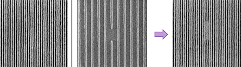
A further advantage of DSA is that it can even repair defects in the guide structures, as is shown in this picture from IMEC.
The big advantage of DSA, if it can be made to work, is that it uses existing equipment. In fact it doesn’t even need the latest generation. It has the potential to be much cheaper than EUV (never mind that EUV might not work out). It reminds me of the first time I heard about CDMA encoding for cell-phones. The idea is elegant but surely in practice, I thought, it will never work. But every phone in Korea and every phone on Verizon uses CDMA. So maybe, one day, every fab will be using DSA. IMEC has the first one already.


Comments
There are no comments yet.
You must register or log in to view/post comments.