You are currently viewing SemiWiki as a guest which gives you limited access to the site. To view blog comments and experience other SemiWiki features you must be a registered member. Registration is fast, simple, and absolutely free so please,
join our community today!
One of the things I really like about major technical conferences is the opportunity to meet with people for networking and interviews. On Wednesday at the Advanced Lithography Conference I had the opportunity to interview Greg Mcinttyre, the director of advanced patterning at IMEC.
IMEC researchers are the first author on 32… Read More
I have previously written about SPIE day 1 and 2 so I want to wrap up my coverage with some impressions from days 3 and 4. My single biggest take away from the conference is that EUV has made tremendous progress in the last 12 months. Last year the mood of the conference was in my opinion pessimistic with respect to EUV, this year the mood… Read More
Imec Technology Forumby Paul McLellan on 04-23-2015 at 7:00 amCategories: Events
I like to quiz people on which country is the one where the most leading edge research on semiconductors is done. People reflexively answer USA or maybe Taiwan or Japan. Nobody who doesn’t already know the answer would pick Belgium. After all the EU headquarters is there not because Belgium is important but because Belgium… Read More
Next week is the SPIE Advanced Lithography Conference in San Jose, the premier conference for advanced lithography used to produce state-of-the-art semiconductors. Last year I blogged after the conference about some of the key points I heard at the conference and this year I plan to do the same.
Last year’s blog is available HERE… Read More
The 40[SUP]th[/SUP] SPIE Advanced Lithography conference will be at the San Jose Convention Center 22-26 February. Over the past few years, this conference has grown in scope to include emerging patterning technologies, like directed self-assembly (DSA) and design-process-technology co-optimization.
Underlying all … Read More
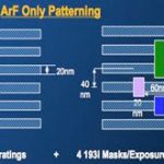
The first part of Lars Liebmann’s ICCAD keynote about lithography was on the changes in lithography that have to us to where we are today. In some ways it was an explanation of why we have the odd design rules, double patterning etc that we have in 20nm and 16nm processes. The second part of his talk was a look forward to how we might… Read More
Round #1 was here.
In the EUV corner were Stefan Wurm of Sematech (working on mask issues mostly) and Skip Miller of ASML who are the only company making EUV steppers (and light sources, they acquired Cymer).
You may know that the biggest issue in EUV is getting the source brightness to have high enough energy that an EUV stepper has … Read More
If you want to know the state of play in lithography, there is no better place than the special session on lithography at Semicon West. This year was no exception. The session was given the punchy title Still a tale of 2 paths: multi-patterning lithography at 20nm and below: EUVL source and infrastructure progress.
In the blue corner… Read More
I will be at Semicon West from 9th to 11th July in Moscone, San Francisco. Of course there are lots of interesting sessions but here are two that I think are especially important to get a good impression of the way things are going in the future from experts. The two most interesting questions about the future are what comes after 14nm,… Read More
Thisblog with a chart showing that the cost of given functionality on a chip is no longer going to fall is, I think, one of the most-read I’ve ever written on Semiwiki. It is actually derived from data nVidia presented about TSMC, so at some level perhaps it is two alpha males circling each other preparing for a fight. Or, in this… Read More