You are currently viewing SemiWiki as a guest which gives you limited access to the site. To view blog comments and experience other SemiWiki features you must be a registered member. Registration is fast, simple, and absolutely free so please,
join our community today!
            WP_Term Object
(
    [term_id] => 1561
    [name] => ESD Alliance
    [slug] => esd-alliance
    [term_group] => 0
    [term_taxonomy_id] => 1561
    [taxonomy] => category
    [description] =>
    [parent] => 386
    [count] => 125
    [filter] => raw
    [cat_ID] => 1561
    [category_count] => 125
    [category_description] =>
    [cat_name] => ESD Alliance
    [category_nicename] => esd-alliance
    [category_parent] => 386
    [is_post] =>
)

WP_Term Object
(
    [term_id] => 1561
    [name] => ESD Alliance
    [slug] => esd-alliance
    [term_group] => 0
    [term_taxonomy_id] => 1561
    [taxonomy] => category
    [description] =>
    [parent] => 386
    [count] => 125
    [filter] => raw
    [cat_ID] => 1561
    [category_count] => 125
    [category_description] =>
    [cat_name] => ESD Alliance
    [category_nicename] => esd-alliance
    [category_parent] => 386
    [is_post] =>
)
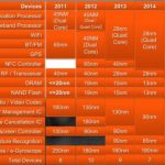
At Semicon Japan a few days ago, Subi Kengeri of GlobalFoundries delivered the keynote. While he covered a number of topics, using Tokyo’s recent win of the 2020 Olympics as a hook, one major theme was the increasing importance of processes other than the bleeding edge digital processes that get all the news.
What is leading… Read More
I should start by saying that SEMI Smart Technology is not technology that is only half as smart as our phones, it is a conference on smart technology organized by SEMI. Officially it is called the International Technology Partners Conference with a sort of subtitle of From Smart Cars to Smart Cities: Shaping the Future of Microelectronics… Read More
With the uncertainties around timing of 450mm wafers, EUV (whether it works at all and when) and new transistor architectures it is unclear whether Moore’s law as we know it is going to continue, and in particular whether the cost per transistor is going to remain economically attractive especially for consumer markets … Read More
There are several events in Silicon Valley coming up of general interest to people working in EDA and the semiconductor industry.
SEMI 16th Annual Valley Lunch Forum. August 22nd, 11.30am to 1.30pm, Santa Clara Marriott
- What are the Opportunities for Advanced Semiconductor Devices?
- Where will the year end for 2013?
- Will we have
…
Read More
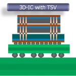
SEMICON Taiwan is September 3rd to 6th in TWTC Nangang Exhibition Hall. Just as with Semicon West in July in San Francisco, there is lots going on. But one special focus is 3D IC. There is a 3DIC and substrate pavilion on the exhibit floor and an Advanced Packaging Symposium. Design tools, manufacturing, packaging and testing solutions… Read More
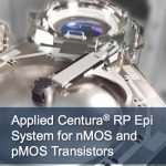
At Semicon I met with Applied Materials to learn about epitaxy. This is when a monocrystalline film is grown on the substrate which takes on a lattice structure that matches the substrate. It forms a high purity starting point for building a transistor and is also the basis of the strain engineering in a modern process.
Since holes… Read More
Round #1 was here.
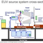
In the EUV corner were Stefan Wurm of Sematech (working on mask issues mostly) and Skip Miller of ASML who are the only company making EUV steppers (and light sources, they acquired Cymer).
You may know that the biggest issue in EUV is getting the source brightness to have high enough energy that an EUV stepper has … Read More
If you want to know the state of play in lithography, there is no better place than the special session on lithography at Semicon West. This year was no exception. The session was given the punchy title Still a tale of 2 paths: multi-patterning lithography at 20nm and below: EUVL source and infrastructure progress.
In the blue corner… Read More
My friend and fellow blogger Kurt Shuler wrote recently, “DAC Is Dead? Long Live DAC!”, which is worth a click over. In addition to providing a nice attendance graph and the top three reasons why it is NOT all rosy, Kurt suggests colocating DAC with other conferences (DESIGN West) but fails to mention SEMICON West.
SEMICON West is … Read More
SEMICON West is next week, July 9-11 in San Francisco. If you haven’t signed up, and want to attend for free instead of $100,
1) Send an email to silicon_test@mentor.com with subject line “Semicon pass.”
2) Register for SEMICON West
3) After registering, download the SEMICON West mobile app and start building your schedule. Here… Read More