In electronic system design, we have grown comfortable with the idea that different regimes of analysis, such as the chip, the package and the system, or electrical, thermal and stress are more or less independent – what starts in one regime stays in that regime, give or take some margin information passed onto other regimes. And why not? It’s worked pretty well for us so far. But now we face a convergence of factors challenging the effectiveness of that decoupling: ADAS expecting significantly longer system lifetimes in more extreme environments, FinFET technologies in which self-heating and Joule heating are becoming more important and wafer-level packaging technologies crowding more electronics into smaller spaces.

Something has to give and what’s giving in this case is the assumption that these factors can be modeled independently. Which is a little scary – now you have to think about modeling heating at the chip, package and system levels across a wide range, from hot-spots on die to a wafer-level package and system enclosures, cooling effectiveness through radiative and convective cooling, and mechanical/stress factors where bonds may break or traces may lift off the interposer or board. Putting all this together requires a broader portfolio of technologies than we commonly expect in EDA.

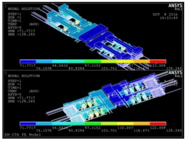
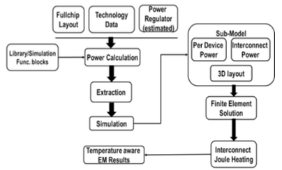
Start with a thermal-aware electromigration (EM) analysis, a factor of great importance to reliability in devices where power level can switch, such as in PMICs or power-managed SoCs. In such cases, higher temperatures mean higher resistance and power-switching means inrush currents through those higher resistance paths, so you have a higher risk of EM. Assuming that massive over-design is not an option, selectively mitigating problem cases requires a fine-grained understanding of heating across the die, which isn’t practical in standard EDA thermal analytics, entering finite-element analysis (FEA). You use traditional methods like FEA to model thermal effects within small, manageable regions and use a variety of methods to minimize / smooth out discontinuities between those regions. All of which helps you understand true temperature exposure at a detailed level. That in turn allows you to manage EM risk at the same level without having to over-design everywhere.

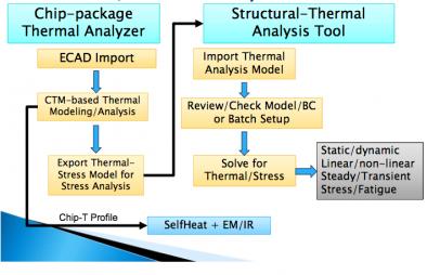
Thermally-induced stress is another important factor for reliability. In wafer-level packaging, as one example, thermal stress on very thin redistribution layers (RDL), popular for thin wafer-level packages, can stress traces, vias and dielectric. Cumulative stress cycling leads to fatigue and therefore reliability problems (increased-resistance in connections or opens). A perhaps lesser-known problem relates to a very significant increase in the coefficient of thermal expansion in dielectrics at something known as the glass transition temperature (Tg). This can lead to significant warpage in the dielectric, especially in WLP, with obvious consequences for reliability. Indeed, especially in WLP, thermally-induced stress analysis becomes particularly important in the highly complex structures found in these technologies, all depending on a variety of materials with unavoidably highly-nonlinear thermal expansion properties.

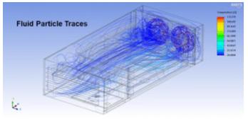
Finally, there’s the small matter of cooling. These are thermal problems after all, so cooling is a part of mitigating those problems. In an ADAS enclosure, modeling the impact of proposed cooling solutions (fans, device positioning, reducing heat from devices) calls for modeling through CFD. Not a chip problem you say? Remember that opening paragraph. We’re building ADAS solutions and they have to be co-optimized in the total package. So yes, CFD modeling is a part of the analysis, perhaps as part of a collaborative development between the Tier 1 and the chip-developer, but each has to be able to exchange models and results to collaborate effectively.
ANSYS unsurprisingly has solutions to these needs, from their chip-package-system (CPS) modeling to their system level thermal and mechanical modeling. You can learn more from work they describe in a paper they presented on thermal-induced stress for fanout wafer-level packaging HERE and a paper they presented on a transient thermal simulation methodology for PMICs HERE.
Share this post via:


Comments
There are no comments yet.
You must register or log in to view/post comments.