




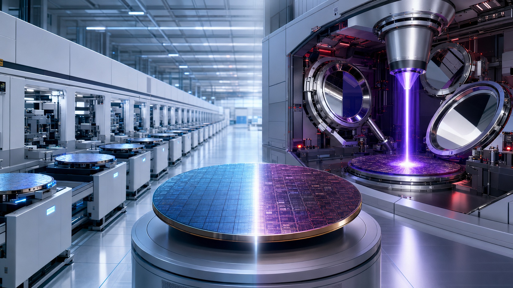

Intel and TSMC are pursuing the same objective—manufacturing smaller, faster, and more energy-efficient semiconductors—but they have adopted different strategies for advanced lithography. Intel moved early to develop High-Numerical-Aperture Extreme Ultraviolet lithography, commonly called High-NA EUV, while TSMC has continued extending conventional EUV for its latest production processes. Their choices reflect different technology roadmaps, manufacturing priorities, and assessments of cost and risk.
Conventional EUV lithography uses 13.5-nanometer light and projection optics with a numerical aperture of 0.33. It has become essential to producing advanced logic chips because it can print much smaller structures than earlier deep-ultraviolet systems. High-NA EUV uses the same wavelength but increases the numerical aperture to 0.55. This enables approximately 1.7 times better resolution and may allow manufacturers to print some critical patterns with one exposure instead of using multiple patterning steps.
Intel became the first chipmaker to receive ASML’s commercial High-NA development system, the TWINSCAN EXE:5000. Installed at Intel’s research facility in Hillsboro, Oregon, the system has been used to develop processes, materials, masks, and design rules for future manufacturing technologies. Intel plans to introduce High-NA EUV into its Intel 14A process, following Intel 18A, while continuing to use conventional EUV and other lithography methods where they offer better economics.
The early commitment supports Intel’s effort to restore semiconductor process leadership and expand its contract-manufacturing business. High-NA EUV gives Intel an opportunity to build expertise before the technology becomes widely used, while potentially simplifying the production of its most critical chip layers. Replacing a multi-patterning sequence with a single exposure could reduce the number of masks and processing steps, shorten manufacturing cycles, and limit errors caused by aligning multiple patterns. Early adoption could therefore provide both a technical advantage and an important point of differentiation for Intel Foundry.
TSMC has followed a more cautious path. The company concluded that it could manufacture its A16 and A14 generations without immediately introducing High-NA EUV into volume production. Instead, TSMC has continued improving its established 0.33-NA EUV platform through better masks, photoresists, overlay control, computational lithography, process optimization, and design-technology co-optimization. Innovations such as nanosheet transistors, backside power delivery, and more flexible standard-cell architectures also provide performance and density improvements that do not depend entirely on lithographic resolution.
Economics are central to TSMC’s decision. High-NA systems are considerably more expensive than conventional EUV scanners and require a new supporting ecosystem. Their anamorphic optics also produce an exposure field only half the size of a conventional EUV field. That limitation can complicate the manufacture of large processors and AI accelerators, potentially requiring two patterns to be stitched together. High-NA also presents challenges involving depth of focus, photoresist performance, masks, inspection, metrology, and yield.
TSMC operates conventional EUV at enormous scale and has accumulated extensive experience maximizing its productivity and reliability. Continuing to use that mature infrastructure reduces execution risk and allows the company to obtain greater returns from its existing equipment.
For an ultra high-volume foundry serving many customers, a proven process with stable yields may be more valuable than introducing the highest-resolution tool before its financial benefits are clear.
This does not mean TSMC has rejected High-NA EUV. The company has purchased equipment for research and has begun developing High-NA lithography technology for future processes. TSMC is ASML’s largest customer, and TSMC CEO C.C. Wei has repeatedly said that the two companies are working closely on High-NA EUV.
TSMC has said that adoption will depend on measurable manufacturing benefits, technology maturity, and cost. Intel is similarly not replacing every conventional EUV exposure with High-NA; it will use the new technology selectively on layers on internal products where its resolution creates sufficient value.
Bottom line: The difference is therefore primarily one of timing. Intel is accepting the cost and risk of being an early adopter in exchange for earlier learning and possible process leadership. TSMC is extending a mature technology while waiting for High-NA EUV to demonstrate stronger production economics. Both strategies may ultimately lead to High-NA manufacturing, but they represent distinct routes toward the next generation of semiconductor scaling.
We’ve discussed this extensively in the SemiWiki Forum, where several lithography experts have weighed in. As always, politically incorrect comments are welcome!
Also Read:
ASML High-NA EUV is Not Ready for High-Volume Production
Crossing the Yield Cliff: IDP V6 and the Future of Manufacturing Forecasting
Beyond Moore’s Law: High NA EUV Lithography Redefines Advanced Chip Manufacturing
Share this post via:



Comments
6 Replies to “Intel and TSMC Take Different Paths to High-NA EUV”
You must register or log in to view/post comments.