You are currently viewing SemiWiki as a guest which gives you limited access to the site. To view blog comments and experience other SemiWiki features you must be a registered member. Registration is fast, simple, and absolutely free so please, join our community today!
Now that semiconductor conferences are virtual there are better speakers since they can prerecord and we have the extra time to do a better job of coverage. Even when conferences go live again I think they will also be virtual (hybrid) so our in depth coverage will continue.
ISSCC is one of the conferences we covered live since it’s in San Francisco so that has not changed. We will however be able to cover many more sessions as they come to our homes on our own time.
First off is the keynote by TSMC Chairman Mark Liu: Unleashing the Future of Innovation:
Given the pandemic related semiconductor boom that TSMC is experiencing, Mark might not have had time to do a live keynote so this was a great opportunity to hear his recorded thoughts on the semiconductor industry, the foundry business model, and advanced semiconductor technologies. Here are some highlights from his presentation/paper intermixed with my expert insights:
The semiconductor industry has been improving transistor energy efficiency by about 20-30% for each new technology generation and this trend will continue.
The global semiconductor market is estimated at $450B for 2020.
Products using these semiconductors represent 3.5% of GPD ($2T USD).
From 2000 to 2020 the overall semiconductor industry grew at a steady 4%.
The fabless sector grew at 8% and foundry grew 9% compared to IDM at 2%.
In 2000 fabless revenue accounted for 17% of total semiconductor revenue (excluding memory).
In 2020 fabless revenue accounted for 35% of total semiconductor revenue (excluding memory).
Unlike IDMs, innovators are only limited by their ideas not capital.
Nothing like a subtle message to the new Intel CEO. It will be interesting to see if the Intel – TSMC banter continues. I certainly hope so. The last one that started with Intel saying that the fabless model was dead did not end so well.
Mark finished his IDM message with:
“Over the previous five decades, the most advanced technology had been available first to captive integrated device manufacturers (IDMs). Others had to make do with technologies that were one or several generations behind. The 7nm logic technology (mass production in 2017) was a watershed moment in semiconductor history. In 2017, 7nm logic, was the first time that the world’s most advanced technology was developed and delivered by a pure-play foundries first, and made available broadly to all fabless innovators alike. This trend will likely continue for future technology generations…”
As we all now know Intel will be expanding TSMC outsourcing at 3nm. TSMC 3nm will start production in Q4 of this year for high volume manufacturing beginning in 2H 2022. The $10B question is: Will Intel get the Apple treatment from TSMC (early access, preferred pricing, and custom process recipes)?
I’m not sure everyone understands the possible ramifications of Intel outsourcing CPU/GPU designs to TSMC so let’s review:
Intel and AMD will be on the same process so architecture and design will be the focus. More direct comparisons can be made.
Intel will have higher volumes than AMD so pricing might be an issue. TSMC wafers cost about 20% less than Intel if you want to do the margins math.
Intel will have designs on both Intel 7nm and TSMC 3nm so direct PDK/process comparisons can be made.
Bottom line: 2023 will be a watershed moment for Intel manufacturing, absolutely!
In its February 20, 2021 edition, the Economist published an article entitled “How to kill a democracy; China faces fateful choices, especially involving Taiwan”. It went on to quote “To many Chinese, the island’s conquest is a sacred national mission” as well as a by-line “America is losing its ability to deter a Chinese attack on Taiwan. Allies are in denial.”
The thought of such an attack should send cold shivers down the chip industry’s spine given, were this to happen, a pivotal part of the western world’s chip supply would dry up overnight. Chip inventories would quickly become exhausted and end equipment production lines everywhere would grind to a halt within a matter of weeks, even days. The near instant impact on global trade and the world economy would be orders of magnitude greater than the 2008 Lehman Brothers crash or the 2020 Covid-19 lockdown.
This problem has been brewing for years, the combined result of an efficient out-sourcing regime, driven faultlessly by TSMC, aided and abetted by super-efficient chip-design tools. Both trends have been manna from heaven to chip firms, users and their investors alike, as it offered lower chip costs and allowed firms to deploy outsourcing-rich, asset-lite manufacturing strategies, increasing profits and diverting their cash flows from investments to dividends and share buy-back schemes. It was accounting Excel Sheet heaven.
No-one paid any attention to the loss of control of a key strategic manufacturing industry, why should they? Taiwan was the West’s friend and TSMC an outstanding company and, in any case, chips were just another commodity. The Real men have fabs’ naysayers were ridiculed as out of touch, out of date, twentieth century dinosaurs.
The current chip shortage, and its devastation impact on the automotive industry, has to a limited extent stirred the chip-supply hornet’s nest, but this will all blow over once the supply-demand imbalance gets sorted. Knee-jerk initiatives, such as US ‘Chips for America’ and EU ‘European Initiative on Processors and Semiconductor Technologies’ are the wrong answer to the right problem. They fail to address the fundamental issue that chip firms do not want to own wafer fabs (it screws up their balance sheet) and the chip users don’t care where the chips come from (so long as they’re cheap). There’s neither market pull or push!
China has been aware of this out-sourced dependency risk for years, hence its drive for national self-sufficiency in chip production, but any fast follower catch-up strategy is notoriously hard to achieve. As a benchmark, it took TSMC over twenty-five years to come close to manufacturing parity with the best in practice manufacturers, and only in the past five has it moved into pole position, yet they are, without doubt, the best chip firm in the world. If it took TSMC this long to catch up, what chance has anyone else, hence the reason why, even before the US-imposed sanctions, China has made such modest progress.
But, as the Economist points out, the Taiwan conundrum represents unfinished business from the 1949 war when the defeated Nationalist regime fled into exile in Taiwan. Were President Xi to fulfil China’s pledge to bring the 23rd Province of China under Communist Party control or not is more a matter of when, not if, with D-Day shaped more by the judgement call whether America would (could?) stop him.
The big question is America’s ability to deter such an invasion, but as America’s starving of chips to Huawei has shown, invasion today no longer entails tanks and troops on the ground, or the streets of Taipei scorched by fire and stained with blood; simply cutting off the electricity and shutting down TSMC’s factories is all it would take to bring America and the rest of the western world to its knees.
For the hawks in China, what better time to do that than now, whilst the non-China world is still struggling with the Covid-19 pandemic, the US democracy and government has been battered by a brutal and divisive presidential election, the world is struggling with a global chip shortage and there is no global consensus whether Taiwan’s independence is worth angering China, especially for some countries, where China is their largest, or a crucial, trade partner.
Taiwan’s recovery back into the Communist fold is not just a sacred national mission, it would also signal that American global leadership had come to an end. The only deterrent is if China feels it cannot complete the task at a bearable cost. Once that fear is reconciled, there is little doubt China will act and, from a chip supply perspective, there will be nothing the rest of the world can do … as the automotive industry has realized, there is no Plan B.
Convergence of Edge Computing, Machine Vision and 5G-Connected Vehicles
Today’s societies are becoming ever more multimedia-centric, data-dependent, and automated. Autonomous systems are hitting our roads, oceans, and air space. Automation, analysis, and intelligence is moving beyond humans to “machine-specific” applications. Computer vision and video for machines will play a significant role in our future digital world. Millions of smart sensors will be embedded into cars, smart cities, smart homes, and warehouses using artificial intelligence. In addition, 5G technology will be the data highways in a fully connected intelligent world, promising to connect everything from people to machines and even robotic agents – the demands will be daunting.
The automotive industry has been a major economic sector for over a century and it is heading towards autonomous and connected vehicles. Vehicles are becoming ever more intelligent and less reliant on human operation. Vehicle to vehicle (V2V) and connected vehicle to everything (V2X), where information from sensors and other sources travels via high-bandwidth, low-latency, and high-reliability links, are paving the way to fully autonomous driving. The main compelling factor behind autonomous driving is the reduction of fatalities and accidents. Realizing that more than 90% of all car accidents are caused by human failures, self-driving cars will play a crucial role in accomplishing the ambitious vision of “zero accidents”, “zero emissions”, and “zero congestion” of the automotive industry.
The only obstacle is vehicles must possess the ability to see, think, learn and navigate a broad range of driving scenarios.
The market for automotive AI hardware, software, and services will reach $26.5 billion by 2025, up from $1.2 billion in 2017, according to a recent forecast from Tractica. This includes machine learning, deep learning, NLP, computer vision, machine reasoning, and strong AI. Fully autonomous cars could represent up to 15% of passenger vehicles sold worldwide by 2030, with that number rising to 80% by 2040, depending on factors such as regulatory challenges, consumer acceptance, and safety records, according to a McKinsey report. Autonomous driving is currently a relatively nascent market, and many of the system’s benefits will not be fully realized until the market expands.
Figure 1 – Automotive AI market forecast for the period of 2017 through 2025
AI-Defined Vehicles
The fully autonomous driving experience is enabled by a complex network of sensors and cameras that recreate the external environment for the machines. Autonomous vehicles process the information collected by cameras, LiDAR, radar, and ultrasonic sensors to tell the car about its distance to surrounding objects, curbs, lane markings, visual information of traffic signals and pedestrians.
Meanwhile, we are witnessing the growing intelligence of vehicles and mobile edge computing with recent advancements in embedded systems, navigation, sensors, visual data, and big data analytics. It started with Advanced Driver Assistance Systems (ADAS), including emergency braking, backup cameras, adaptive cruise control, and self-parking systems.
Fully autonomous vehicles are gradually expected to come to fruition following the introduction of the six levels of autonomy defined by the Society of Automotive Engineers (SAE) as shown in Figure 2. These levels range from no automation, conditional automation (human in the loop) to fully automated cars. With increasing levels of automation, the vehicle will take over more functions from the driver. ADAS mainly belongs to Level 1 and Level 2 of automation. Automotive manufacturers and technology companies, such as Waymo, Uber, Tesla, and a number of tier-1 automakers, are investing heavily in higher levels of driving automation.
Figure 2 – Levels defined by SAE for autonomous vehicles
With the rapid growth of innovations in AI technology, there is a broader acceptance of Level 4 solutions, targeting vehicles that mostly operate under highway conditions.
Although the barrier between Levels 3 and Level 4 is mainly regulatory at this time, the leap is much greater between Levels 4 and 5. The latter requires achieving the technological capability to navigate complex routes and unforeseen circumstances that currently necessitate human intelligence and oversight.
As the automation levels increase, there will be a need for more sensors, processing power, memory, efficient power consumption, and networking connectivity bandwidth management. Figure 3 shows various sensors required for self-driving cars.
The convergence of deep learning, edge computing, and the Internet of vehicles is driven by the recent advancements in AI automotive and vehicular communications. Another enabling technology for machine-oriented video processing and coding in visual data applications and industries is the emerging MPEG Video Coding for Machine (MPEG-VCM) standard. Two specific technologies are investigated for VCM:
Efficient compression of video/images
The shared backbone of feature extraction
Powerful AI accelerators for inferencing at the edge, standard-based algorithms for video compression and analysis for machines (MPEG-VCM), and 5G connected vehicles (V2X) play a crucial role in enabling the full development of autonomous vehicles.
The 5G-V2X and emerging MPEG-VCM standards enable the industry to work towards harmonized international standards. The establishment of such harmonized regulations and international standards will be critical to global markets of future intelligent transportation and AI automotive industry.
There are a number of possible joint VCM-V2X architectures for the future autonomous vehicle (AV) industry. Depending on the requirements for the given AV infrastructure scenarios, we can have either centralized, distributed, or hybrid VCM-V2X architectures as shown in Figure 4. Currently, most connected car automaker manufactures are experimenting with the centralized architecture with low-cost cameras. However, as the cameras become more intelligent, distributed, and hybrid architectures due to their scalability, flexibility, and resource sharing capabilities can become more attractive. The emerging MPEG-VCM standard also provides the capability of transporting the compressed extracted features rather than sending compressed video/images between vehicles.
Gyrfalcon Technology Inc. is at the forefront of these innovations by using the power of AI and deep learning to deliver a breakthrough solution for AI-powered cameras and autonomous vehicles — an unmatched performance, power efficiency, and scalability for accelerating AI inferencing at the device, edge, and cloud level.
The convergence of 5G, edge computing, computer vision, and deep learning, and Video Coding for Machine (VCM) technologies will be key to fully autonomous vehicles. Standard and interoperable technologies such as V2X, emerging MPEG-VCM standard, powerful edge, and onboard compute inferencing accelerator chips enable low-latency, energy-efficient, low-cost, and safety benefits to the demanding requirements of the AI automotive industry.
About Manouchehr Rafie, Ph.D.
Dr. Rafie is the Vice President of Advanced Technologies at Gyrfalcon Technology Inc. (GTI), where he is driving the company’s advanced technologies in the convergence of deep learning, AI Edge computing, and visual data analysis. He is also serving as the co-chair of the emerging Video Coding for Machines (VCM) at MPEG-VCM standards. Prior to joining GTI, Dr. Rafie held executive/senior technical roles in various startups and large companies including VP of Access Products at Exalt Wireless, Group Director & fellow-track positions at Cadence Design Services, and adjunct professor at UC Berkeley University. He has over 90 publications and served as chairman, lecturer, and editor in a number of technical conferences and professional associations worldwide.
Functional Verification for complex ASICs or IP-Core products is a resource limited ‘quest’ to find as many bugs as possible before tape-out or release. It can be a long, difficult and costly search that is constrained by cost, time and quality. The search space is practically infinite, and 100% exhaustive verification is an unrealistic and non-tractable problem. The goal is to deliver the highest possible quality (measured by both product performance and absence of bugs), achieving that in the shortest possible time (in order to maximise revenue), with the lowest possible costs.
Complexity continuously increases, and the functional verification challenge gets progressively harder. The search gets longer, and the bugs become increasingly more difficult to find. In practice, some bugs will be missed because verification is inherently imperfect and non-exhaustive. How do you find most of the bugs? How do you find all of the critical bugs? In “The Origin of Bugs” we asserted that:
Verification is a resource limited ‘quest’ to find as many bugs as possible before shipping.
Terms of Reference
So, what makes verification more challenging than other aspects of engineering when developing complex semiconductor products? Take other design workflows of semiconductor development such as RTL synthesis, timing analysis, place and route, power analysis and sign-off checks. As a rule, these workflows tend to be reasonably deterministic. They may consume significant engineering resources (skilled people and compute), but there is usually a well-defined process to converge or iterate towards a result. When you get there, there is a measurable degree of completeness in the results. We’re generalizing of course. There are challenges and uncertainties with these workflows, but with verification the $64,000 question is always “Am I done yet?”. We don’t believe we can answer the verification sign-off question with the same degree of certainty as the design implementation sign-off. We also know that the consequences of missed critical bugs, can be potentially catastrophic. See “The Cost of Bugs” for a more detailed discussion on the cost of “not finding bugs”.
We characterize this verification uncertainty as the following set of dilemmas that need to be carefully navigated; completeness, complexity, constrained-random, resources and delivery.
The Completeness Dilemma
Verification is not an exact science. There is no way to achieve completeness or perfection. You have to decide when you have done enough work that you are satisfied that the risk of critical bugs remaining in the design is acceptably and manageably low.
Verification is an exercise in risk mitigation.
The problem comes down to the impossibly large state space in almost all modern ASICs. It’s a non-tractable problem. You might also think of this as the
“impossibly large state-space dilemma!”
This is also related to the complexity-dilemma which we will discuss in the next section.
Some sense of completeness can be achieved when verification targets have been met. Verification becomes a data-driven quest; it’s all about metrics and analysis, with verification sign-off driven by the assessment of metrics such as coverage, test-pass rates, cycles since last bug, cycles since last RTL change, formal properties proven, bug rates, etc. All of these sign-off criteria should be captured in the “test plan” and reviewed, revised and approved. You’re looking for a convincing absence of bugs despite measurable efforts to find further bugs in an RTL code base that has been stable for an acceptable period of time. You can’t be too complacent. The bugs are still in there. Your efforts so far have failed to find them!
All of your verification efforts will suffer from the completeness dilemma.
Take test planning, which is the normal starting point. The process to develop the test plan is one of design and specification analysis, brainstorming, reviewing, and iterative refinement. It’s probably the most important step; sometimes undertaken at the beginning of the project, sometimes evolving over time in a more agile fashion. Either way, it is impossible to develop complete test plans. Late found bugs can usually be traced back to a shortfall in the test plan, maybe a missing corner case, or even a gap where a whole class of behaviors have been omitted from the test plan.
Take coverage, which is commonly relied upon as a good measure of the completeness of verification stimulus. Code coverage does give some sense of absolute measure in that every line of RTL code and every branch and expression has been visited during testing. However, it does not inform us that functionality is correct, or about missing lines of code i.e., missing functionality. We know that code coverage is just one measure. Commonly teams will be using functional coverage to measure stimulus in terms of its ability to exercise functional behaviors observed as events or sequences or more complex combinations and crosses of coverage. These functional coverage points collectively form the “coverage model”, but how do you know that the coverage model is complete? Like test planning, it is another “best-effort” exercise that relies on a process of analysis and review, refinement and iteration. You may still omit an important functional coverage point which (had it been present) would have exposed a critical gap in your stimulus that was hiding a critical bug. Best to always assume,
If it’s not tested, it’s broken!
The same applies to most other aspects of verification. Even formal verification, where you might think there is some promise of completeness (by exhaustively proving properties) is an incomplete science. Many properties cannot be exhaustively proven, only shown to not fail for a given depth of cycles (bounded proofs). You have the same issue with your formal properties as you do with functional coverage and stimulus – how do you know for certain that you have planned and implemented a complete set of properties?
Ditto for system-level verification/system validation. You will not know that your testing payloads are complete and that they will be able to find all of the remaining bugs that were missed by previous levels of verification.
Sadly, some bugs will be missed.
Those hidden bugs might never present in the field over the lifetime of the product, meaning that the product is fit for purpose and therefore meets its requirements. However, you can’t be certain of what code from the software ecosystem will eventually run on your system. Software development tools may change over time and may produce different code sequences that were not present in the testing payloads at the time of verification sign-off. All of this runs the risk that eventually a previously unseen dark corner-case will be encountered with unpredictable consequences, potentially occurring for the first time in the field. If you are lucky, there may be a viable and deployable software mitigation that does not significantly degrade performance or function, in which case, you got away with it! If you are unlucky and no such software mitigation is possible, you may be looking at a hardware mitigation or a costly product update. Again, see “The Cost of Bugs” for a more in-depth discussion about cost impacts of hardware bugs.
So, this lack of completeness is a dilemma for the developer of complex ASICs or IP-Cores. It is something to be constantly aware of and something to be considered at length when reasoning about the age-old question,
“Am I done yet?”
The Complexity Dilemma
The key causes of the completeness dilemma are the “impossibly large state-space” dilemma and the complexity dilemma. ASIC or IP-Core products only ever get more complex, they seldom deliver more capabilities by being simpler. We’re talking about complex hardware components or sub-systems such as CPUs, GPUs, ML/AI processors, integrated into multi-core SoCs and ASICs that may be multi-billion gate devices. For verification, it’s a good result if tools, methodologies and platform performances and capacities can at least keep up with complexity growth, let alone getting ahead of it. That’s the dilemma. Engineering teams need to understand complexity and curtail it wherever they can, but at the same time complexity is necessary to achieve performance, capabilities and ultimately, competitive advantage. Complexity that is introduced to achieve performance and functional goals, is often harder to contain, and design teams are always innovating new architectures and microarchitectures that will set their product apart from the competition in terms of performance and functional capabilities.
Furthermore, complexity is not something that you may have set out to achieve. A once clean and elegant design can degrade over time into something containing a lot of technical debt, as the code is iterated and reworked, optimized and re-factored, potentially by multiple individuals over the lifetime of the development.
When the code author admits that they really no longer have a complete understanding, it’s time to panic!
Think about strategies to contain design complexity wherever possible. Reduce it by refactoring code, purging redundant code, and maintaining code readability and maintainability. Investigate suitable metrics to measure complexity if possible.
The Constrained-Random Dilemma
Over recent decades, constrained-random verification methodologies have become the norm. Given our understanding of the completeness dilemma (which means we acknowledge that it is impossible to identify all possible testing scenarios) random testing offers a way to find scenarios we had not specified thanks to “random chance”. The probabilities of hitting these unknown scenarios are increased by volume of testing.
If we run enough cycles, we will eventually hit it… probably, we hope!
But this philosophy has hugely driven up verification platform costs, and oftentimes we don’t really have a good understanding of how effective all those random cycles are at finding these unknown-unknowns. Of course, there is more to it than that. This is not a fully random strategy, it is ‘constrained-random’. We identify constraints for the stimulus generators to guide stimulus into specific areas of interest. We then use ‘coverage’ methods to measure the effect of the stimulus, and stimulus-generators and coverage models are refined over time. However, this strategy eventually leads to a saturation point, where we are no longer finding new bugs and are now running ‘soak’ cycles to build confidence and assurances that a “respectable” (you have to decide what that is) volume of bug-free testing has been achieved. Determining what this safe assurance level is can be difficult and you may be required to justify exceedingly large engineering costs based on your judged targets and analytics.
How do you know if you have sufficient constraints? Over-constraining means you might be missing some key areas of stimulus where bugs could be hiding. You might not realize that because your coverage model is not complete either! Some bugs may require pathological sequences that are just too improbable for the generator to produce. If you can identify these cases, you might be able to program them into your generator – but that requires you to realize that these cases exist. Shared learning from experience and historical projects can really help here.
Constrained-random suffers from the completeness dilemma and the resources dilemma.
The Resources Dilemma
How do you deliver the product on-time and to the right quality level?
You had better make sure that you are using the available resources in the most efficient and effective way possible.
At the risk of repeating ourselves, but let’s anyway…
Verification is a resource-limited quest to find as many bugs as possible before release.
Server racks with telecommunication equipment in server room
Resources are always finite and limited, regardless of whether your resources are on-prem or in the cloud. On-prem implies investment costs to establish infrastructure and development tool capacity, and then ongoing operational costs to operate and maintain the platforms. Cloud implies that there are some cost constraints or budget parameters that you have to operate within. If your capacity demand changes, there will be additional costs of acquisition and commissioning, but there is likely to be an availability lag as it inevitably takes time to expand on-prem capacities. If you are already using cloud to provision your infrastructure, the availability lag may not be there, but the incremental usage costs will be.
Let’s not forget the human resources side of this equation. Team sizes can flex, but people costs are the biggest resource cost in general, and you have to deliver your product within the constraints of the available team. Make sure that your teams have the right skills profile, the best tools, and are well-motivated and engaged, because staff turnover can be one of the most disruptive things to occur mid-project.
Engineering teams have to use the resources that are available to them, in the most effective and efficient way, to achieve the best verification results possible within these constraints.
Sometimes these constraints help to drive engineering innovation to improve the efficiency and effectiveness of verification workflows. How do we achieve better Quality of Results (QoR), from the same or less resources, in the same or less time, thus reducing the cost of verification and increasing product ROI? In our experience, engineers love to innovate, so direct them towards these challenging problems. After all,
Scarcity of resources, drives innovation.
Optimization is a never-ending quest that requires you to measure everything. Optimize your workflows; optimize your tools and select the ones with the best performance; profile and optimize your testbenches and verification code to make them run as efficiently as possible.
Securing resources for your project is oftentimes a process of negotiation. Good resource forecasting is essential to ensure you have planned ahead for the resource demand, but these forecasts need to be reviewed and refined throughout the project. If you are competing for shared resources, human behavior can lead to negotiation tactics, e.g., figure out what you think you need and add a buffer or sandbag your estimates by an amount that you think you will be negotiated back down by! Forecasting really needs to be a transparent and data-driven process where predictions are accurate and based on best-practice analytics.
Conclusion – the Delivery Dilemma
Finally, you have to deliver your product on time and on cost. Endlessly polishing the product beyond the point where the documented goals and sign-off criteria are met will erode the product ROI and left un-checked can destroy it. Remember…
Perfection is the enemy of success.
The delivery dilemma can lead to some tough calls on occasions. It’s a matter of risk management. This is where you have to be very clear about what your sign-off criteria are and how you are measuring up against them. You started with good intentions and a comprehensive test plan, but now you need to assess status. Look at all the data and make a judgement call on the remaining risk. You can think of this signoff in terms of “must do”, “should do”, “could do”, and
“Things that will help you to sleep better at night!”
By the time you get here you have probably achieved all of the first three items and are making a judgment call on the fourth. Consider the following:
Delaying the final release will block resources; people and infrastructure, that are needed to execute on the delivery of other revenue bearing projects and the overall business roadmaps.
Delaying the final release will increase the product cost and erode ROI.
Delaying the final release will have a downstream impact on the customer’s schedules, which in turn impacts their ROI (and potentially your future opportunities).
Get this wrong however, and you might incur substantial rework costs, opportunity costs, and reputational costs, as a consequence of an impactful bug!
Having made the release, there is still a window of opportunity where you could continue to make marginal improvements to the verification so that any new bugs can be intercepted and mitigated before the product is widely deployed into the field. As verification engineers, we know that some level of extended background verification can be a good investment of engineering resources, especially if we are still in a pre-silicon situation.
The real challenge is in deciding when to stop!
Although this paper does not prescribe solutions to these dilemmas, having an understanding of them can help in navigating good verification choices.
Dan and Mike are joined by Ray Zinn, the longest serving CEO in Silicon Valley. Join us for a tour of the very beginnings of the semiconductor industry and the rise of the fabless movement. Beyond a historical perspective, Ray also discusses the importance of semiconductor technology and its impact on the world, governments and the US in particular.
“As the longest serving CEO in Silicon Valley, it is now my mission to enlighten, encourage and guide the next generation of entrepreneurs.”
The views, thoughts, and opinions expressed in these podcasts belong solely to the speaker, and not to the speaker’s employer, organization, committee or any other group or individual.
It has been my pleasure to interview Graham Curren, CEO of Sondrel. A veteran of the Electronics Design industry, he founded Sondrel in 2002 to provide digital ASIC designs.
How did you aim to differentiate Sondrel when you started?
My view of the market was that there were a lot of small design companies and also huge in-house design teams. There was a gap that would grow as chips would only become more complex taking them out of the skill and price range of many companies. I founded Sondrel with the aim of being able to take on the design of a chip that would need teams of engineers working for a year or more and provide some economy of scale.
How well did that work out?
Badly to start with, because it was at the end of the dotcom boom (or the start of the bust). However, over time, things improved and, over the last 18 years, we’ve grown at an average of around 25% every year. We had to grow, of course, to be able to reach the staffing levels so we could handle design contracts for big digital chips. In fact, we are one of the few companies in the world with the staff and expertise to tackle such enormous projects – apart from those with in-house design teams.
How big are we talking?
We are regularly designing large chips, such as a recent one of 500 square millimetre chip that has over 30 billion transistors, 40 million flipflops, and 23 thousand pads for I/O, power and ground.
That would be beyond the skills of many in-house design teams!
Exactly. Which is why customers come to us as we have the experience of designing the architecture of big chips and solving the many associated challenges such as the NoC (Network on Chip), timing issues between different parts of the chip and between different chiplets for a SIP design, etc. As we have solved these challenges on many different chips, we provide a low risk means to get to market faster. Part of this success is that engineering teams have access to the rest of the 200 plus engineers working for Sondrel to brainstorm for ideas, additional skills and experience.
Do you only do big chips?
It is our speciality; however, we are doing some smaller devices now in response to customer demand since we are offering a full turnkey service of design through product validation to shipping silicon. This is really exciting existing customers and bringing in new customers who want the security of a one-stop shop for their product creation in silicon.
Why are you offering turnkey services?
Defining and designing a chip for a customer means that we really get to know them and what they want their chip to do and we are able to bring some of the advanced process techniques to the older generation nodes. This can have a big impact on things like testing, minimising test time and field test failures which are a very expensive but often under-represented part of the design process. For these customers we become a trusted partner.
The supply chain is a complex process to manage with many opportunities for mistakes that could result in costly delays. So many customers told us horror stories about the less advanced supply chain support that they had received that we decided to solve it by offering a full turnkey ASIC service to take responsibility for the whole process from the initial brief for the chip, designing the ASIC and then managing the supply chain process right to shipping the tested silicon chips to customers. We are the single point of contact managing everything giving opportunities to improve the chip as time moves on, for example by improving the test to catch more failures. This means that customers can now focus all their energies on their area of expertise and innovation, safe in the knowledge that we will deliver the silicon to turn their ideas into real products.
Any other design specialities apart from big designs?
Of course, all designs in the latest technologies have huge numbers of transistors and therefore can be considered big! Designs can have Giga numbers of transistors and yet the actual size is in the square millimetres. Which is why we often describe them as complex chips and that what we do as a company is to make complexity simple.
We are very skilled at supporting the newer technologies – almost everything we do is below 28nm going right down to 5nm. Then there are design domains such as low power and high security where we have long established expertise. Functional safety and radiation hard are two examples of the new exciting areas that we are working on with clients.
All these different areas provide the variety that our designers really like as it enables them to learn new skills. That really attracts engineers to join us as we are big enough to have the latest tools and innovations, yet small enough that individuals’ ideas are listen to and can make a real difference to projects.
Sondrel is very well known in Europe and Asia but much less so in the USA. Why is that?
Growing a company organically has to be done at the right speed. Too fast and you can’t manage it (and you run out of cash). Too slow and others take your market share. We are headquartered in the UK so naturally our first focus was Europe. Then Asia as we have offices there with design engineers so it was logical to have sales teams there too based in our largest market in the region – Xi’an, China.
2021 is the year that we are really starting to build our presence in the US starting with Silicon Valley. A year ago, we took on Dave Krishna as VP of Sales and Marketing, North America. He is a great guy and so well connected that he is finding projects despite the COVID lockdown. We have now welcomed others to the team and have expanded our sales and technical support locally both in southern California and on the east coast. We are looking to continue to grow this team rapidly with positions for engineers and business development experts.
How has COVID affected Sondrel?
Fortunately, hardly at all. Unlike many design companies that have teams of people in offices as the only way to operate, a couple of years ago we ensured that all our staff have the ability to work effectively from home with fast, secure internet connections to our servers. As lockdowns were imposed in the various countries round the world that we operate in, we simply closed that office and the staff started working from home the next day. It helps that we have more senior, experienced staff that don’t have to be closely supervised to do their work. As a result, not a single customer project has been delayed, and we are receiving enquiries from customers who have been let down by our rivals who could not cope with lockdowns.
That’s great forward planning!
The ability to work from home is just one of the things that we have in place to make Sondrel a great place to work. I’m a firm believer that happy staff work better and are committed to go that little bit extra if needed. It certainly showed by the way that everyone pulled together to cope with all the issues of the pandemic.
What else do you do for staff?
We have always had flexible working hours for good work/life balance, which helped when staff had to also become teachers for their children locked down at home. Another big thing is the Social Committee that every office has and organises events from paintball to family picnics and from bowling to flower arranging. These events help bond us into a big family. Even during lockdown, they were organising quiz nights to keep people in touch with one another. Despite many requests, we have yet to manage a virtual curry night!
Are you finding it hard to recruit in the lockdown?
Not really. It has become quite apparent how different we are to rivals in terms of working arrangements, some of whom are insisting that staff have to come into offices and not work from home. As a result, engineers are approaching us to join. Fortunately, we recruiting for staff in all our offices around the world – China, USA, UK, France, Morocco and India. Our target is to recruit over a hundred engineers this year.
Why so many?
As I mentioned, our systems were already in place for home working. Some rivals really struggled and let customers down. They are turning to us with projects as we have proven to be a very safe, reliable partner so 2021 is looking very good for us. Which is why we need many more engineers to service this dramatic increase in business.
SoC designers often have to make a, “red pill or blue pill,” decision when it comes to selecting process technology. Usually, a choice has to be made between performance, power and area, with one being prioritized at the expense of the others. However, as is pointed out in a recent paper by Mixel and NXP, designers can have the best of both worlds – the red pill and the blue pill – if they consider using a fully depleted silicon on insulator (FD-SOI) process. This is especially true because FD-SOI comes with an extensive ecosystem in the form of tool support and IP availability.
FD-SOI has been a niche technology compared to bulk CMOS, but with new demands from applications like IoT for low standby power and analog & digital performance, it may be ripe for a renaissance. In the paper titled “It’s Time to Look at FD-SOI (Again)” by Eric Hong, senior director of engineering at Mixel, and Nik Jedrzejewski, product line manager at NXP Semiconductors, they make the point that FD-SOI offers unique features that make it an excellent choice for IoT.
Mixel and NXP have worked together to provide designers a superior alternative to bulk CMOS processes. The paper highlights the NXP i.MX 7ULP platform for 28 FD-SOI which leveraged Mixel’s MIPI D-PHY IP.
Let’s look at what the authors have to say about the performance characteristics of FD-SOI devices. FD-SOI places an oxide insulation layer the under the entire transistor, which uses a thin channel with raised source and drain material. This construction provides for many interesting properties that can be exploited to improve chip design. This configuration reduces parasitics and short channel effects.
In bulk CMOS there is parasitic capacitance between the source, drain and the substrate. Also, in bulk CMOS two effects, gate-induced drain leakage (GIDL) and drain-induced barrier lowering (DIBL) play havoc with threshold voltage and high drain voltage turn-off, respectively. With FD-SOI, on the other hand, the buried oxide (BOX) layer shields the source & drain and allows for a thinner channel, improving the gate’s ability to turn off. The reduction of gate and parasitic capacitances mean that peak and dynamic power are reduced, and transconductance and ft are improved.
FD-SOI Advantages
Perhaps the most interesting property of FD-SOI is that body-biasing of the substrate under the junction can easily be applied. This body biasing can even be modified dynamically depending on the operating characteristics needed at the time. To improve the already impressively low stand-by leakage, reverse body-biasing (RBB) can be applied. The authors report that leakage can be reduced by up to a factor of 50X with this technique.
By applying forward body-biasing (FBB), the threshold voltage can be lowered, allowing for improved performance and higher gate overdrive (Vdd-Vt). The authors mention cases where there has been more than a 60% performance improvement with a 1V supply. Mixel observed a power savings of 50% on a design at the fast corner (FF). The same design saw a 14% power reduction at the typical corner (TT). This was accomplished with a W/L reduction of 55% for the on-chip devices. Body biasing can also be used to compensate for die-to-die variations to improve yield.
The paper also includes details about how FD-SOI improves many of the performance characteristics of transistors when they are used in analog design. This alone makes reading the entire article worthwhile. FD-SOI offers not one, but many advantages for designs seeking to improve power, performance, area and yield.
NXP, working with Mixel, have assembled a very compelling platform for SOC design based on FD-SOI. The paper also includes a diagram showing the combined IP and blocks available for building application processors. There is a complete and well-established ecosystem ready to go for designers facing challenges with using bulk CMOS processes for their products. To get the full picture, read the paper here for more information.
Effective and efficient functional verification is one of the biggest hurdles for today’s large and complex system-on-chip (SoC) designs. The goal is to verify as close as possible to 100% of the design’s specified functionality before committing to the long and expensive tape-out process for application-specific integrated circuits (ASICs) and full custom chips. Field programmable gate arrays (FPGAs) avoid the fabrication step, but development teams still must verify as much as possible before starting debug in the bring-up lab. Of course, verification engineers want to use the fastest and most comprehensive engines, ranging from lint, static and formal analysis to simulation, emulation and FPGA prototyping.
However, leading-edge engines alone are not enough to meet the high demands for SoC verification. The engines must be linked together into a unified flow with common metrics and dashboards to assess the verification progress at every step and determine when to tape out the chip. The execution of all the engines in the flow must be managed in a way to minimize project time, engineering effort and compute resources. Verification management must span the entire length of the project, satisfying the needs of multiple types of teams involved. It must also provide high-level reports to project leaders to help them make critical decisions, including tape-out. This article presents the requirements for effective SoC verification management.
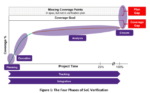
Phases of Verification
There are four significant phases of verification: planning, execution, analysis and closure. As shown in Figure 1, these phases can be viewed as linear across the project’s duration. In a real-world application, the verification team makes many iterative loops through these phases. Identification of verification holes during the analysis phase may lead to additional execution runs or even revisions to the verification plan. Similarly, insufficient results to declare verification closure and tape out may ripple back to earlier phases. This is a normal and healthy part of the flow, as verification plans and metrics are refined based upon detailed results.
A unified flow and intelligent decision-making throughout the project require tracking verification status and progress in all four phases. Also, there are multiple points where the verification flow must integrate with tools for project and lifecycle management, requirements tracking and management of cloud or grid resources. Figure 1 also shows the two major gaps that must be closed before tape-out. The coverage gap represents the verification targets identified during the planning phase but not yet reached during the execution phase. The plan gap refers to any features in the chip specification not yet included in the verification plan. The verification team must close both gaps as much as possible.
Planning Phase Requirements
The verification plan lies at the heart of functional verification. At one time this was a paper document listing the design features and the simulation tests to be written for each feature to verify its proper functionality. The verification engineers wrote the tests, ran them in simulation and debugged any failures. Once the tests passed, they were checked off in the document. When all tests passed, verification was deemed complete and project leaders considered taping out. This approach changed with the availability of constrained-random testbenches, in which there is not always a direct correlation between features and tests.
In an executable verification plan, engineers list the coverage targets that must be reached for each feature rather than explicit tests. They may use constraints to aim toward specific features and coverage targets with groups of tests, but it is a much more automated approach than traditional verification plans. Coverage targets may exist in the testbench or the design and may include code coverage, functional coverage and assertions. Verification planning includes determining which engine will be used for which features. Simulation remains the primary method. Still, formal analysis, emulation and other verification engines might be more appropriate for some targets.
As shown in Figure 2, the verification plan features must be linked directly to content (text, figures, tables, etc.) in the design specification. This reduces the chances of features being missed since specification reviews will reveal any gaps in the verification plan. The plan must be kept in sync with the specification so that the verification team can see whether goals are being met at every phase of the project. The planning phase springboards from this plan, defining milestones for progress toward 100% coverage. Coverage tends to grow quickly early in the project but converges slowly as deep features and corner cases are exercised. Results from all engines must be aggregated intelligently and then back annotated into the verification plan so that the team has a unified view of achieved coverage and overall verification progress.
Execution Phase Requirements
Once the initial plan is ready, the verification team must run many thousands of tests, often on multiple engines, trying to reach all the coverage targets in the plan. This must be highly automated to minimize the turnaround time (TAT) for each regression test run, which will occur many times over the project. Whenever a bug is fixed or additional functionality is added to the design, the regression is executed again. Regressions must also be re-run whenever changes are made to the verification environment. An efficient solution requires an execution management tool that initiates jobs for all verification engines, manages these jobs, monitors progress and tracks results.
As illustrated in Figure 3, ordering and scheduling of tests are critical to minimize the TAT. Tests must be distributed evenly across all the grid or cloud compute resources so that the regression run uses as much parallelism as possible. Also, the information from each regression run can be used to improve the performance of future runs. The analysis phase must be able to rank tests based on coverage achieved. This information is used by the execution management tool in the next run to skip any redundant tests that did not reach any new coverage targets. This makes regressions shorter and makes better use of compute resources, storage space and verification engine licenses, all of which are managed by the same tool.
Coverage data is considered valid only for tests that complete successfully. Of course, many times tests will fail due to design bugs or errors in the verification environment. Most project teams execute regressions without debug options such as dump file generation to reduce regression runtime. The execution management tool must detect each failing test and automatically rerun it with appropriate debug features enabled. The engine must collect pass/fail results and coverage metrics so that they can be analyzed in the next phase of verification.
Analysis Phase Requirements
Once all tests have been run in the execution phase, the verification team must analyze the results to determine what to do next. This consists of two main tasks: debugging the failing tests and aggregating the passing tests’ coverage results. Access to an industry-leading debug solution is critical, including a graphical user interface (GUI) with a range of different views. These must include design and verification source code, hierarchy browsers, schematics, state machine diagrams and waveforms. It must be possible to cross-probe and navigate among the views easily, for example, selecting a signal in source code and seeing its history in a waveform. Once the reason for a test failure is determined, it is fixed and then verified in the next regression run.
Aggregating the coverage results can be tricky because different verification engines sometimes provide different results. Formal analysis can provide proofs of assertions and determine unreachable coverage targets, which simulation and emulation cannot. The verification team may also define custom coverage metrics that must be aggregated with the standard types of coverage. The aggregation step must be highly automated, producing a unified view of chip coverage. The coverage results and other data from the regression runs must be stored in a database and tracked over time, as shown in Figure 4. Verification trends are a crucial factor in assessing project status, projecting a completion date and making the critical tape-out decision.
The analysis phase must include test ranking by contribution to coverage to reduce the TAT for regression runs in the execution phase. Deeper analysis begins as the verification team examines the coverage holes that occur when the passing regression tests do not yet reach coverage targets. The verification engineers should study the unreachable targets identified by formal analysis carefully to ensure that design bugs are not preventing access to some of the design’s functionality. Aggregating unreachability results improves coverage metrics and prevents wasting regression time on targets that cannot be reached. This is another way to reduce execution TAT by making efficient use of cloud and grid resources.
Closure Phase Requirements
Once the verification engineers have eliminated coverage targets formally proven unreachable, as shown in Figure 5, they must consider the remaining targets not yet reached by the regression tests. Coverage closure is the process of reaching these targets or excluding them from consideration. If the verification engineers decide that a coverage target does not need to be reached, it can be added to an exclusions list. The analysis engine must support adaptive exclusions to be persistent even if there are small changes in the design. Reaching a coverage target may involve modifying existing tests, developing additional constrained-random tests, writing directed tests or running more formal analysis.
Modifying tests usually entails tweaking the constraints to bias the tests toward the unreached parts of the design. The results are more predictable if the closure phase supports a “what-if” analysis, in which the verification engineers can see what effect constraint changes will have on coverage. Ideally, this phase results in 100% coverage for all reachable targets. In practice, not all SoC projects can achieve full coverage within their schedules, so the team sets a lower goal that is typically well above 95%. The goal must be high enough to make managers feel confident in taping out and to minimize the chance of undetected bugs making it to silicon.
Tracking Process Requirements
Effective and efficient SoC verification requires the ability of the verification team and project management to observe results during any of the four phases and to track these results over time. Information from every regression run and analysis phase should be retained in a database so that both current status and trends over time can be viewed on-demand. The verification management flow must generate a wide variety of charts and reports tailored to the diverse needs of the various teams involved in the project.
Integration Process Requirements
There are many tools used in the SoC development process beyond the verification engines and the verification management solution. Information in the verification database must be exported to these other tools; other types of data may be imported. Many development standards mandate the use of a requirements management and tracking system. The features in the specification and verification plan must be linked to the project requirements. The verification management solution must also link to project management tools, product lifecycle tools and software to manage cloud and grid resources. Finally, verification engineers must be able to integrate with custom tools via an open database and an application programming interface (API).
Summary
Verification consumes a significant portion of the time and expense of an SoC development project. The planning, execution, analysis and closure phases must be automated to minimize resource requirements and reduce the project schedule. This article has presented many key requirements for these four phases and two critical processes that span the project. Synopsys has developed a verification management solution that meets all these requirements and is actively used on many advanced chip designs. For more information, download the white paper.
HCL Compass is quite a powerful tool to accelerate project delivery and increase developer productivity. Last August I detailed a webinar about HCL Compass that will help you understand the benefits and impact of a tool like this. This technology falls into the category of DevOps, which aims to shorten the systems development life cycle and provide continuous delivery with high software quality. Scalability across the enterprise is a key factor for success here, so cloud migration is definitely a consideration. Recently, I detailed how HCL is assisting its users to get to the Amazon Elastic Compute Cloud. Vendor choice is definitely a good thing. I’m happy to report that HCL expands cloud choices with a comprehensive guide to Azure deployment.
Microsoft Azure, commonly referred to simply as Azure is a major force in cloud computing. Moving any enterprise application to the cloud provides significant benefits, including:
Lower costs
Increased agility
Reliable global delivery
There are some specific impacts that HCL’s migration guide cites (a link is coming). Some of these are worth repeating:
Cost effectiveness: VMs (virtual machines) deployed in the cloud remove the capital expense of procuring and maintaining equipment as well as the expense of maintaining an on-premises data center. These VMs can host instances of HCL Compass
Scalability: Estimating data center capacity requirements is very difficult. Over-estimation leads to wasted money and idle resources. Under-estimation degrades the business’s ability to be responsive. Cloud computing resources can easily and quickly be scaled up or down to meet demand. Of particular interest regarding this point, Azure provides autoscaling that automatically increases or decreases the number of VM instances as needed
Availability: Azure, like other cloud providers, invests in redundant infrastructure, UPS systems, environmental controls, network carriers, power sources, etc. to ensure maximum uptime. Most enterprises simply cannot afford this kind of scale
The guide from HCL provides everything you need to plan your HCL Compass deployment or migration in Azure. There’s a lot of items to consider, so having all this in one place is very useful. Here are just a few of the considerations that are addressed in the HCL guide:
Supported database platforms: Ensuring you are using the correct version of the required database software is key. Versions between on-premises and the cloud are discussed, along with recommendations on how to utilize an on-premises database for a cloud deployment. This latter discussion supports a hybrid environment.
Accessing the data: For a cloud deployment, the preferred method of data access is to utilize the HCL Compass web client. The specific browsers and versions to use are specified, along with the cautions and pitfalls of other approaches.
Requisite software: Along with Linux database versions, the required versions for installation software, Java, Windows and Linux are discussed.
Many other topics are explained in detail, including:
Performance and performance monitoring
Cross-server communication
Load balancing
SSL enablement
Single sign-on implementation
LDAP authentication
Multi-site implementation
EmailRelay considerations
A detailed discussion of migration considerations is also presented, along with sample implementation scenarios. One scenario treats HCL Compass and the database in Azure. The other treats HCL Compass in Azure with the database on-premises. All-in-all, this guide provides a complete roadmap to implement HCL Compass in Azure. I can tell you from first-hand experience that cloud migration can be challenging. Software is provisioned and managed differently in a cloud environment. As long as you understand those nuances, things go smoothly.
The migration guide provided by HCL helps you discover all those nuances. You can get your copy of this valuable guide here. Download it now and find out how HCL expands cloud choices with a comprehensive guide to Azure deployment.
The views, thoughts, and opinions expressed in this blog belong solely to the author, and not to the author’s employer, organization, committee or any other group or individual.
Is it possible to find and prioritize holes in coverage through AI-based analytics on coverage data? Paul Cunningham (GM, Verification at Cadence), Jim Hogan and I continue our series on research ideas. As always, feedback welcome.
Improving coverage starts with knowing where you need to improve, especially where you may have significant holes. Getting to what you might call good scalar coverage (covered functions, statements, and the like) is fairly mechanical. Assertions provide a set of more complex checks on interdependencies, high value but necessarily low coverage. These authors look at cross-product checks, relationships between events, somewhat reminiscent of our first blog topic.
It is important first to understand what the authors means by a cross-product coverage task. This might be say a <request,response> pair where <request> may be one of memory_read, memory_write, IO_read, IO_write and <response> may be ack, nack, retry, reject. Coverage is then over all feasible combinations.
Events are assumed related through naming. In their convention, reg_msr_data_read breaks into {reg,msr,data,read} which is close to {reg,msr,data,write}, not quite as close to {reg,pcr,data,write}. (You could easily adapt to different naming conventions.) From these groups they run K-means clustering analysis to group features (reg, msr, etc).
From these clusters, they build cross-product structures. This starts with sets of feature locations, counting from start and end of an event. Then finding anchors, most commonly occurring, and therefore likely most significant features in events (reg for example). The authors call groups of features falling between these anchors dimensions. Though not quite explicit in the paper, it seems these provide a basis for probable event combinations which ought to be covered. From that they can then monitor covered and non-covered events. Better yet, they can provide very descriptive guidance on which combinations they expected to see covered but did not.
Paul’s view
The depth of this paper can be easy to miss on a quick read. It’s actually very thought provoking and draws on ML techniques in text document classification to help with verification. Very cool!
The verification methodology in this paper is based on “coverage events” represented as a concatenation of words, e.g. “reg_msr_data_read”. However, the paper would seem to be equally applicable to any meta-data in the form of semi-structured text strings – it could be debug messages for activity on a bus or even the names of requirements in a functional specification.
The heart of the paper is a set of algorithms that cluster similar coverage events into groups, break apart the concatenation of words and then intelligently re-combine the words to identify other concatenations that are similar but as yet un-covered events. They use a blend of K-means clustering, non-negative matrix factorization (NMF), and novel code to do this. The paper is a bit thin on specifics of how K-means and NFR are applied, but the essence of the overall method still shines through and the reported results are solid.
The more I think about this paper, the more the generality of their method intrigues me – especially the potential for it to find holes in a verification plan itself by classifying the names of functional requirements themselves. The approach could quite easily be added as an app to a couple of the coverage tools in our Cadence verification flow…a perfect opener for an intern project at Cadence – please reach out to me if you are reading this blog and interested.
Jim’s view
Paul made an interesting point (separately). At the block level people are already comfortable with functional coverage and randomization. But at the SoC level, Engineers typically use directed tests and don’t have as good a concept of coverage. They want functional coverage at SoC but it’s too much work.
Maybe this is a more efficient way to get a decent measure of coverage. If so, that would definitely be interesting. I see it as an enhancement to existing verification flows, not investable as a standalone company, but certainly something that would be interesting as a quick acquisition. This would follow a proof of concept of no more than a month or so – a quick yes/no.
My view
Learning techniques usually focus on pure behaviors. As Paul suggests, this method adds a semi-semantic dimension. It derives meaning from names which I think is quite clever. Naturally that could lead to some false positives, but I think those should be easy to spot, leaving the signal to noise ratio quite manageable. Could be a nice augment perhaps to PSS/ software-driven verification.