This is another installment covering TSMC’s very popular Open Innovation Platform event (OIP), held on August 25. This event presents a diverse and high-impact series of presentations describing how TSMC’s vast ecosystem collaborates with each other and with TSMC. The topic at hand was full of superlatives, which isn’t surprising when Cerebras and Analog Bits talk about how they effect collaboration on the largest and most powerful AI chip in the world.
The presentation began with Dhiraj Mallick. vice president engineering and business development at Cerebras Systems. Dhiraj introduced Cerebras as an exciting AI systems startup with a mission to transform the landscape of compute by accelerating a new class of workloads like AI orders of magnitude over today’s state-of-the-art. Dhiraj discussed the challenges of tasks such as deep learning training. He explained that compute requirements for these types of workloads have increased 300,000-fold over the past eight years. This equates to a doubling every 3.4 months. Those who follow Moore’s Law will realize how significant this acceleration is.
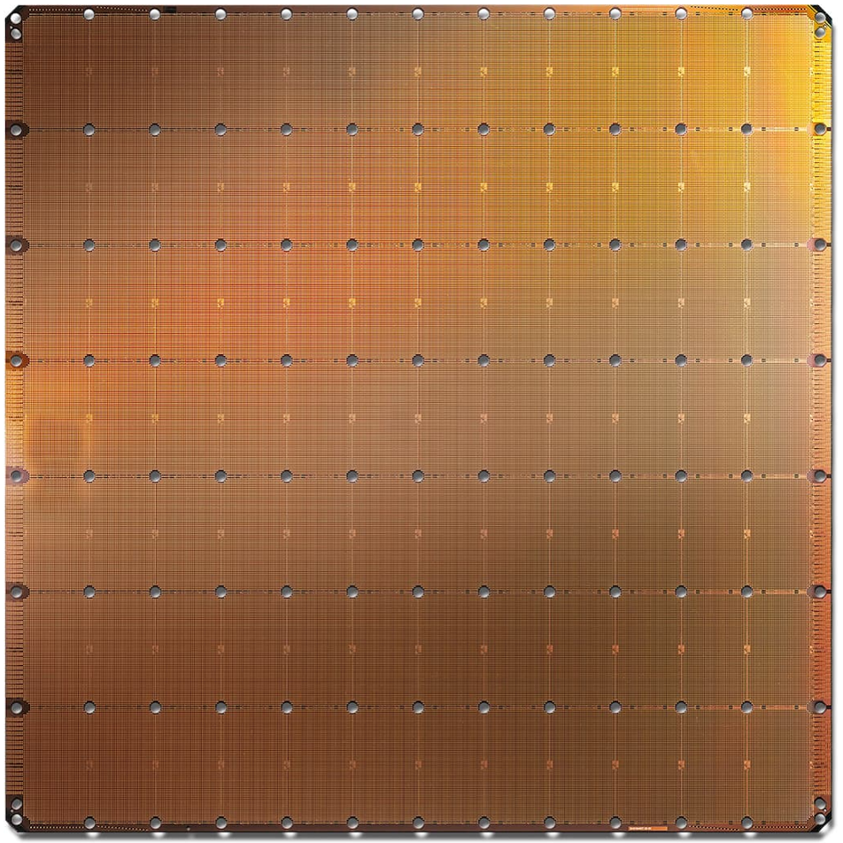
To address this problem, Cerebras has built the world’s largest processor. The statistics of this chip, pictured above, are mind-boggling. The chip is over 46,000 mm2 in size, equivalent to about 60 reticle-limited chips. It contains 400,000 cores, all fully programmable and optimized for deep learning and sparse linear algebra. The chip contains 18 GB on-chip SRAM with unprecedented memory bandwidth and a mesh system for core-to-core communication capable of 100 Pb/s. When you are collaborating on the largest and most powerful AI chip in the world, everything is record-breaking.
Dihraj went on to discuss the challenges of power integrity with a design like this. He explained that hundreds of thousands of independent cores on a single piece of silicon result in dynamic current surges causing die voltages to exceed functional limits. System performance consequences can include catastrophic failures. The approach Cerebras chose to address this challenge was to use an analog glitch detection circuit from Analog Bits. These devices have a real-time response and 840 of them were distributed over the Cerbras wafer-scale chip. Dihraj explained a significant advantage of the Analog Bits IP was its ability to detect anomalies with much higher bandwidth than digital approaches, resulting in true real-time identification of power integrity events. The benefits of the Analog Bits solution can be summarized as follows:
- High-precision, real-time power supply monitoring IP exceeding 5pVs sensitivity
- Fully integrated analog macro that interfaces to a digital SoC environment
- Highly user programmable for trigger voltages, depth of glitch, time-span of glitches
- The ability to monitor multiple thresholds simultaneously, providing a wealth of data to optimize the instantaneous current spike suppression and overall effectiveness
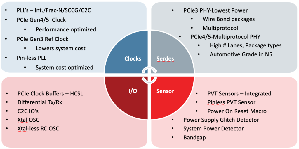
Dihraj then introduced Mahesh Tirupattur, executive vice president at Analog Bits to cover more details about Analog Bits IP and collaboration with TSMC. Mahesh began with an overview of the various Analog Bits IP that address clocking, I/O, sensing and serial communication. He explained that Analog Bits takes a system view of problem solving. The figure below summarizes their offerings.

Mahesh then focused on the company’s sensor technology. Their on-die PVT sensor monitors voltage, temperature and process in one block. An integrated power on reset monitor is also available, as well as a power supply glitch detector. This last block was developed in collaboration with their customers, including Cerebras. It measures voltage spikes as well as voltage drops. This block has some unique features, as summarized below:
- Integrated voltage reference for precision stand-alone operation
- Easy to integrate with no additional components or special power requirements
- Easy to use and configure
- Cascadable for up to 4 additional glitch detection channels
- Independent programming available for glitch detection levels
- Low power
- Implemented with Analog Bits’ proprietary architecture
- Requires no additional on-chip macros, minimizing power consumption
Mahesh then elaborated on more of the unique capabilities of the glitch detector IP. He then provided silicon results of five corner lots at extreme voltage conditions, both trimmed and untrimmed. Regarding the roadmap, the glitch detector IP is silicon-proven in TSMC’s 7FF process, with N5 available in Q3-2020 and N3 available in Q1-2021. In addition, Analog Bits is working on a system power supply detection macro in TSMC N5. This IP provides synchronous detection with latched outputs. It also offers a programmable droop detection level. It will be available in Q3-2020.
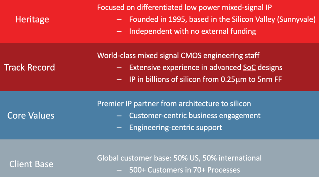
Mahesh closed with some comments about the collaboration between TSMC and Analog Bits, which dates back to 2004. Several test chips have been done as a result of this collaboration. He described an N7 test chip done last year that included 5 corner split lots, with exhaustive characterization reports available and IP 9000 certification. Mahesh concluded with some corporate background on Analog Bits, as summarized below. The collaboration between Cerebras and Analog Bits to create the largest and most powerful AI chip in the world was quite impressive. To learn more, visit the Analog Bits website.

Also Read:
AI processing requirements reveal weaknesses in current methods
7nm SERDES Design and Qualification Challenges!
CEO Interview: Alan Rogers of Analog Bits
Share this post via:


Comments
One Reply to “Cerebras and Analog Bits at TSMC OIP – Collaboration on the Largest and Most Powerful AI Chip in the World”
You must register or log in to view/post comments.