RVN! 26 Banner revised (800 x 100 px) (600 x 100 px)

System Technology Co-Optimization (STCO)

System Technology Co-Optimization (STCO)
by Daniel Payne on 11-30-2021 at 10:00 am

An early package prototype

My first exposure to seeing multiple die inside of a single package in order to get greater storage was way back in 1978 at Intel, when they combined two 4K bit DRAM die in one package, creating an 8K DRAM chip, called the 2109. Even Apple used two 16K bit DRAM chips from Mostek to form a 32K bit DRAM, included in the Apple III computer, circa 1978. So the concept to assemble multiple die into a single package has been around for decades now. The new name for this methodology is System Technology Co-Optimization, or STCO for short, because system-level engineers are now combing memory, processors, mixed-signal IP and sensors into single packages.

Some electronic systems can be built on a single SoC economically, while other system approaches are using packaging techniques in order to interconnect multiple, specialized die, yielding lower costs than a monolithic approach. With multiple die involved, there is a new challenge in how to optimize such a system.

Per Viklund at Siemens EDA wrote a white paper on this topic, and I’ll share the highlights in this blog. Chiplets are being used to save costs over a single SoC implementation, and the interconnect is through High Density Advanced Packaging (HDAP) approaches with 2.5D and 3D stacked die. Prototyping is recommended for STCO success, to ensure that the effects of power integrity, signal integrity, thermal, warp and mechanical stress are understood before production begins.

An early package prototype

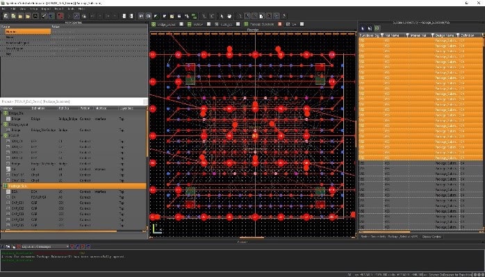
Waiting for all of the chiplets to be designed, and then starting the packaging design process is much too late in the schedule to make any partitioning trade-offs, so the preferred approach is to start the package design quite early as a package prototype. The idea is to iterate on several alternative package prototypes when it’s possible to impact the partitioning of features into each chiplet. At the earliest stage of package prototype there may be few details per chiplet, but the idea is to incrementally add more information.

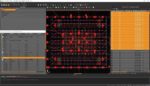
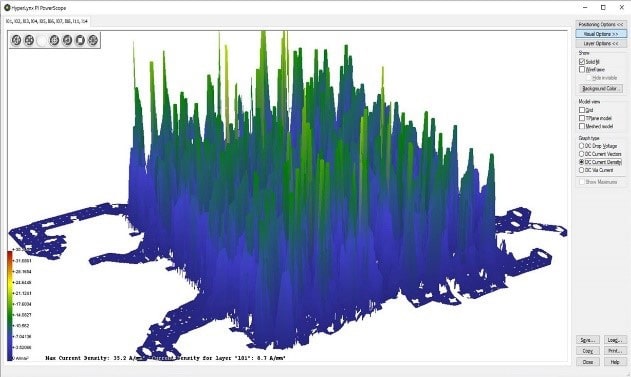
Even with a package prototype it’s possible to run early analysis of power integrity and signal integrity.  An early model has approximate chiplet sizes and the interconnect signals, so using power integrity tools an engineer can determine how many power and ground bumps are needed for the package as a first pass to spot any issues.

Power integrity simulations

With the package prototype methodology it’s possible to run early simulations to uncover and fix issues with mechanical stress, warping, die attachment and metal cracking. As each chiplet is completed, then more detailed analysis can replace the earlier prototype results. There’s also a final, 3D fully assembly verification, to make certain that there are no surprises.

Summary

There is a methodology for System Technology Co-Optimization (STCO), applied to chiplet-based designs, which involves creating a prototype package early in the system design process, then running early analysis, and to start making partitioning trade-offs. Physical effects are considered early in the prototyping process, and multi-physics analysis finds and fixes any issues.

This is another example of shift left, applied to system projects using HDAP. To read the complete, seven page White Paper, Using a System Technology Co-Optimization (STCO) Approach for 2.5/3D Heterogeneous Semiconductor Integration, visit the Siemens EDA site, and provide some basic information to download.

Related Blogs


High-Performance Natural Language Processing (NLP) in Constrained Embedded Systems

High-Performance Natural Language Processing (NLP) in Constrained Embedded Systems
by Kalar Rajendiran on 11-30-2021 at 6:00 am

Demonstrator Block Diagram

Current technology news is filled with talk of many edge applications moving processing from the cloud to the edge. One of the presentations at the recently concluded Linley Group Fall Processor Conference was about AI moving from the cloud to the edge. Rightly so, there were several sessions dedicated to discussing AI and edge processing software and hardware solutions. One of the presentations within the Edge IP session was titled “High-Performance Natural Language Processing in Constrained Embedded Systems.” The talk was given by Jamie Campbell, software engineering manager at Synopsys.

While the bulk of data nowadays is generated at the edge, most of it is sent to the cloud for processing. Once the data is processed, applicable commands are sent back to the edge devices for implementing the applicable action. But that is changing fast. Within a few years, a majority of the data is expected to be processed at the edge itself. The drivers for this move are reduced latency, real-time response requirement, data security concerns, communication bandwidth availability/cost concerns, etc., The applications demanding this are natural language processing (NLP), RADAR/LiDAR, Sensor Fusion and IoT. This is the backdrop for Jamie’s talk which focuses on NLP in embedded systems. He makes a case for how NLP can be efficiently and easily implemented in edge-based embedded systems. The following includes what I gathered from this Synopsys presentation at the conference.

Jamie starts off by introducing NLP as a type of artificial intelligence which gives machines the ability to understand and respond to text or voice. And he classifies natural language understanding (NLU) as a subtopic of NLP which is focused on understand the meaning of text. The focus of his presentation is to showcase how an NLP application can be implemented within an embedded system.

Embedded System Challenges

As fast as the market for edge processing is growing, the performance, power and cost requirements of these applications are also getting increasingly demanding. Embedded systems within edge devices handle specific tasks, balancing accuracy of results at power/performance/area efficiencies. The challenge is to select algorithms appropriate for implementing those tasks, execute within the constraints of the embedded systems and still deliver the performance and accuracy needed. Choosing the optimal execution models and implementation hardware is key, whether it is an NLP application or any other application within embedded systems.

Demonstration of NLP Implementation

Jamie explains the project that they embarked on at Synopsys is to demonstrate that a useful NLP system can be implemented in a power constrained, low-compute-capacity environment. The use case they chose is an automotive navigation application that can be operated through natural language commands. The goal is to understand queries such as “How far is it from suburbs to city center” and “is road from city center to suburbs icy.” The expected output from the application are two things: Intent and Slots. Intent defines what is needed to execute the query. Slots are qualifiers that augment the Intent. In the case of the two sample queries stated above, the intent is “Get Distance” and the slots are the “Waypoints”. The application is to extract intent and slots from the text output derived from automatic speech recognition (ASR).

The demonstration system uses a 3-step process for the NLP implementation. The three steps are

  • Audio feature extraction
  • Automatic Speech Recognition (ASR)
  • Intent and Slots Recognition

Selecting the Models

For the audio feature extraction, the widely used voice recognition algorithm (MFCC feature extraction technique) was chosen.

For the ASR and conversion to text, the QuartzNet ASR Model was chosen as it requires a lot less memory (~20MB) than many of the other models considered. It delivers a good Word Error Rate (WER) and it does not require a language model to augment the processing.

For the intent and slots which is the NLU step, a lightweight LSTM encoder-decoder model was chosen. 

Selecting the Libraries and Hardware

While there are many processors to choose from, the Synopsys VPX processor family was selected for use in the embedded NLP demonstration project. The VPX family implements a next-generation DSP architecture optimized for a data centric world and is well suited for NLP use cases. An earlier blog covers lots of details of the functionality and features of the VPX processor family. Following is an excerpt from that blog to explain the choice of the VPX processor for this use case demonstration project.

“Earlier this year, Synopsys announced an expansion of its DesignWare® ARC® Processor IP portfolio with new 128-bit ARC VPX2 and 256-bit ARC VPX3 DSP Processors targeting low-power embedded SoCs. The announcement was about their VPX DSP family of processors for Language processing, Radar/LiDAR, Sensor Fusion and High-end IoT applications. In 2019, the company had launched a 512-bit ARC VPX5 DSP processor for high-performance signal processing SoCs.  The ARC VPX processors are supported by the Synopsys ARC MetaWare Development Toolkit, which provides a vector length-agnostic (VLA) software programming model. From a programming perspective, the vector length is identified as “n” and the value for n is specified in a define statement. The MetaWare compiler does the mapping and picks the right set of software libraries for compilation. The compiler also provides an auto-vectorization feature which transforms sequential code into vector operations for maximum throughput.

In combination with the DSP, machine learning and linear algebra function software libraries, the MetaWare Development Toolkit delivers a comprehensive programming environment.”

Implementation

For convenience, Synopsys uses a PC-based host along with a HAPS® FPGA platform for implementing the NLP-based automotive navigation demonstration. All of the processing happens on the HAPS platform where the VPX5 processor is implemented. The demonstration shows that real-time performance is achieved on a 30MHz FPGA system. If this use case were to be implemented with an ASIC, a VPX2 processor can easily meet the performance requirements. And with the VLA programming model supported through the MetaWare Development Toolkit, customers can easily migrate from a VPX5 to a VPX2 implementation.

Conclusion

Migrating an NLP/NLU application from a powerful cloud server environment to a standalone, deeply-embedded system is possible without sacrificing real-time performance and without requiring lot of memory resources. The choice of the neural network models selected and the hardware chosen to implement the solution play a big role in successful migration to the edge. To learn more about the VPX DSP processors, you can visit the product page.

Also read:

Lecture Series: Designing a Time Interleaved ADC for 5G Automotive Applications

Synopsys’ ARC® DSP IP for Low-Power Embedded Applications

Synopsys’ Complete 800G Ethernet Solutions


Siemens EDA will be returning to DAC this year as a Platinum Sponsor.

Siemens EDA will be returning to DAC this year as a Platinum Sponsor.
by Daniel Nenni on 11-29-2021 at 10:00 am

Siemens EDA DAC

The 38th Design Automation Conference is next week and this one is for the record books. Having been virtual the last two years, next week we will meet live once again. I think we may have all taken for granted the value of live events but now we know how important they are on both a professional and human level, absolutely.

“The Design Automation Conference (DAC) is recognized as the premier conference for design and automation of electronic systems.  DAC offers outstanding training, education, exhibits and superb networking opportunities for designers, researchers, tool developers and vendors.”

“We would like to extend a big thank you to the DAC organizers under the leadership of Siemens EDA’s own Harry Foster, the General Chair of this year’s Design Automation Conference, in organizing a wonderful conference program under challenging circumstances. Kudos, Harry and the DAC program team!” – Siemens EDA Management

Siemens EDA in the Conference Program

You’ll find Siemens EDA experts featured throughout the conference program – delivering five conference papers and four DAC Pavilion presentations, hosting a tutorial and designer track panel, and presenting 11 posters during the Poster Networking Reception. We’ve highlighted some must-see events below, but you can view their full list of conference activities here.

DAC Pavilion Session: Digitalization—the return to outsize growth for the semiconductor industry

10:15am – 11:15am PST | Monday, Dec. 6th

Joe Sawicki, Executive VP of Siemens EDA

In just one short year, a decade of digitalization occurred across all industries fueled by innovation in the semiconductor industry. Dramatic growth occurred in use of the cloud, work from anywhere and telemedicine, while online collaborative tool usage increased a staggering 4000%.

Impressive as this all is, it is just the beginning of a massive reinvigoration of the semiconductor industry. Emerging new compute and telecom infrastructures, with IoT starting to deliver its long-promised value, coupled with new technologies such as artificial intelligence are reshaping the competitive landscape at break-neck speed. Despite valid concerns over trade wars, there is no doubt the semiconductor market is once again on a dramatic growth trajectory.

Designer Track Panel: UVM: Where the Wild Things Are

10:30am – 12:00pm PST | Wednesday, Dec. 8th

Moderator: Dennis Brophy, Siemens EDA

Experts from Cerebras, Marvell Semiconductor, NVIDIA, Paradigm Works, and Synopsys will focus on specific enhancements being planned or considered to be added for the next revision of UVM IEEE 1800.2. Panelists have strong backgrounds in UVM development as current or past members of the UVM-WG in Accellera and/or IEEE and equally strong opinions on what is needed to keep UVM growing and relevant for functional verification.

Tutorial: Design and Consumption of IPs for Fail: Safe Automotive ICs

1:30pm – 5:00pm PST | Monday, Dec. 6th

This tutorial featuring experts from Siemens EDA, NXP Semiconductors, and Arm Ltd. will focus on both the creation and consumption of automotive IP, looking at the various technologies and methodologies that can be used to standardize and automate this process.

Must-See Conference Paper Presentations:

Input Qualification Methodology Helps Achieve System Level Power Numbers 8x Faster

An automated Input Qualification Methodology is proposed that performs various Data Integrity Checks at design build and prototype stage and ensures in quicker iterations that input data is high fidelity leading to a well correlated power numbers. If multiple retries are needed, checkpoint database method is implemented to bypass the clean stages of the tool run.

Various checks pertaining to activity annotation (FSDB/SAIF/STW/QWAVE), technology libraries (.lib) and parasitic (SPEF) mapping are already part of the tool. Defining an input qualification methodology around these checks can save up to 88% of project time in achieving reliable power numbers.

What can chip design learn from the software world?

Many industries are undergoing a major transformation in the last years, but it seems the chip design practice is still basically where it was decades ago, with relatively minor improvements since. On the other hand, new bigger projects enabled by the on-going Moore’s law race, pose increasingly harder design & verification challenges – that our industry is struggling to keep up with.

It seems that our friends in the software industry also face big challenges, but they have been introducing many and different approaches, methodologies, technologies to do things different…and better. We will discuss the need and possibility of doing things different and potentially better, looking at certain concepts from the software development world and look into some possible concepts that could be adopted more broadly, such as: Open Source, Agile methodology and leveraging data and machine learning.

Siemens EDA customers will be delivering presentation and posters at DAC on their use of Siemens EDA technologies.

Customer presentations include:

Customer poster sessions include:

DAC Design Infrastructure Alley Presentation: Siemens EDA Cloud Offerings

3:30pm – 4:15pm PST | Monday, December 6th

Watch Craig Johnson’s presentation at the Design on Cloud Theater to learn how Siemens EDA is leading the way in cloud-based EDA.

Siemens EDA on the Exhibit Floor

You can visit Siemens EDA experts on both exhibit floors of Moscone West. The main Siemens EDA booth (#2521) is on the second floor – stop by to grab a free espresso drink and tune in to our informative booth presentations. You can also find them in the booths for OneSpin, A Siemens Business (#1539), Siemens Cloud (#1246), and Siemens at RISC-V Pavilion, booth B7.

Also Read:

Machine Learning Applied to IP Validation, Running on AWS Graviton2

Siemens EDA Automotive Insights, for Analysts

Tessent Streaming Scan Network Brings Hierarchical Scan Test into the Modern Age


Silicon Catalyst Hosts an All-Star Panel December 8th to Discuss What Happens Next?

Silicon Catalyst Hosts an All-Star Panel December 8th to Discuss What Happens Next?
by Mike Gianfagna on 11-29-2021 at 6:00 am

Silicon Catalyst Hosts an All Star Panel December 8th to Discuss What Happens Next

Each year, Silicon Catalyst assembles a panel of industry luminaries to discuss important questions about the future. The charter of the Silicon Catalyst Industry Forum is to: “create a platform for broad-topic dialog among all stakeholders involved in the semiconductor industry value chain. The Forum topics focus on technical and financial aspects of the industry, but more importantly the industry’s societal, geo-political and ecological impact on the world. “

Last year, for Forum 3.0, “A View to the Future” was pondered. You can view coverage of that event here and replay the complete 2020 Forum here.  The fourth annual version of this event is happening on December 8.

Once again for 2021, it’s a seasoned and high-profile cast who will participate. The event promises to be both entertaining and thought-provoking. After the year we’ve all just experienced, the topic seems particularly on-point:

Semi Industry Forum 4.0: What happens next?


The panel will be moderated by Don Clark, Contributing Journalist, New York Times. Panel members includeMark Edelstone, Chairman of Global Semiconductor Investment Banking at Morgan Stanley; Janet Collyer, Independent Non-Executive Director, UK Aerospace Technology Institute; John Neuffer, President & CEO, Semiconductor Industry Association; and Dr. Wally Rhines, President & CEO of Cornami and GSA 2021 Morris Chang Exemplary Leadership award recipient. Quite a group of industry luminaries.

Panelists

The event will begin with a Forum 4.0 overview from Richard Curtin, Managing Partner at Silicon Catalyst. Pete Rodriguez, CEO of Silicon Catalyst will then introduce the panel and Mark Edelstone will kick things off with a presentation of the on-going semiconductor industry consolidation. A panel discussion will then follow moderated by Don Clark.

As a backdrop for the panel discussion, the semiconductor industry, and society in general, is now at a major inflection point. The globalization of the supply chain, combined with the on-going geo-political turmoil, layered on top of the pandemic, has created a unique set of challenges for our industry, and most importantly, the world at large.

Topics to be discussed during the panel include:

  • Semiconductor Supply Chain Challenges: The current limited supply situation has impacted all aspects of our lives, industries, and global economies. Is there an end in sight? What are the key lessons learned? What should be done to ensure that the current chip shortage and other supply chain challenges are not repeated in the future?
  • US-China Relationship: The recent trend of punch / counterpunch does not seem to have an end in sight. As viewed by both countries, our industry is “too big to fail”. We’re now well beyond risk-mitigation and squarely in crisis-mode. Can we ever put the “genie back in the bottle?”
  • Public-Private Partnerships vs Free-Market Forces: The response to the pandemic has clearly shown that industry and government can collaborate for the good of society. Can the same be said for the initiatives by the major industrialized nations to establish domestic sources for the vital electronics demanded by their industries and societies? Is it too little, too late? And what impact will the continuing consolidation of semiconductor vendors, combined with local government investments, drive a new type of “territorial bottom-line”?
  • Startups: The landscape for startups has changed substantially over the past decade. What are the new challenges chip startups face? What barriers must be overcome? What target markets and applications are most promising?
  • Work-From-Home: The Good, the Bad and the Ugly: WFM / hybrid work environments are here to stay, especially for those in that are in the “knowledge worker” demographic. If you’re an electronic systems vendor, you’re seeing record setting business results (if you can get the chips…). But isn’t the history of the semiconductor industry’s innovation significantly based on the “randomness” of chance encounters with colleagues in the office? Can we truly be as creative and innovative, working individually dispersed and remote?

Silicon Catalyst’s Semiconductor Industry Forum 4.0 will take place on December 8, 2021, at 9:00 AM Pacific time. You can register for the event here.  You’ll want to attend this event to better understand what happens next.

Also Read:

Silicon Startups, Arm Yourself and Catalyze Your Success…. Spotlight: Semiconductor Conferences

WEBINAR: Maximizing Exit Valuations for Technology Companies

Silicon Catalyst and Cornell University Are Expanding Opportunities for Startups Like Geegah


Big Data Helps Boost PDN Sign Off Coverage

Big Data Helps Boost PDN Sign Off Coverage
by Tom Simon on 11-28-2021 at 8:00 am

PDN Sign Off

The nearly unavoidable truth about dynamic voltage drop (DVD) signoff for power distribution networks (PDN) is that the quality of results depends on the quality and quantity of the vectors used to activate the circuit switching. As SOCs grow larger and are implemented on smaller nodes, the challenges of sufficient coverage and increased sensitivity of chips to PDN issues makes the task of PDN sign off increasingly difficult. Often designers are limited to only running a few nanoseconds of vectors due to runtime and capacity issues. Western Digital recently gave a presentation at the Ansys Ideas Digital Forum on the how they used the capabilities in Ansys® Redhawk-SC™ with the SeaScape Analysis Platform to achieve big improvements in PDN Sign off coverage. The presentation, given by Kushang Bajani, principal engineer at Western Digital, is titled “A Methodology for Steep Increase in PDN Sign-off Coverage Using Big-Data Platform”.

Western Digital switched to Redhawk-SC from Redhawk to take advantage of the native cloud support and big-data techniques it offers. SeaScape allows RedHawk-SC to utilize scalable parallel processors and distributed local memory for running extremely large jobs. Previously for each vector set and mode the user needed to create and maintain a separate set-up. Thanks to the massive parallelization offered with SeaScape, many vector sets can be run in parallel to find the most comprehensive worst case switching for power. Redhawk-SC can consolidate the worst power windows from multiple vector sets to provide a realistic worst case for sign off.

PDN Sign Off

In his experience, Kushang reports seeing runtime going from 60 hours to just 12 hours in a multi VCD flow. This actually also allowed increased coverage and in one test case RedHawk-SC uncovered a better power window that had double the power usage of the one they found using just Redhawk.

To ensure that they felt comfortable moving to Redhawk-SC, Western Digital ran an exhaustive correlation exercise to verify QoR. Kushang shares one example where they started with a 4.034 microsecond VCD. Both tools identified the same 10 ns power window. When they ran each tool to get power figures they matched within a fraction of a percent.

Kushang feels that they now have significantly improved PDN sign off coverage. This comes with improved runtimes that make it possible to screen using multiple vectors, even on large multi-million node designs. They can uncover more potential PDN weaknesses and have higher confidence when they go to tape-out.

SeaScape is a key enabling technology for RedHawk-SC, giving it the ability to run much larger design problems and explore PVT conditions, modes and vectors. The results can be combined using analytics to provide insights into the design. SeaScape scales linearly to hundreds of CPUs and can operate on-premises or in the cloud. For many companies having the ability to access massive compute resources only as needed means that high costs of ownership can be avoided.

RedHawk-SC is the first application that Ansys has ported to the SeaScape platform, but others, like PathFinder-SC, are also available now and others to follow soon. We’ve always known that EDA’s compute requirements are very large. Ansys’ investment in offering their users a pathway to efficiently, reliably, and easily access resources to improve design results is good to see. The full presentation by Western Digital is available on-demand by registering at the Ansys IDEAS Digital Forum.

Also Read

Optical I/O Solutions for Next-Generation Computing Systems

Bonds, Wire-bonds: No Time to Mesh Mesh It All with Phi Plus

Neural Network Growth Requires Unprecedented Semiconductor Scaling


Empyrean Technology‘s Complete Design Solution for PMIC

Empyrean Technology‘s Complete Design Solution for PMIC
by Daniel Nenni on 11-28-2021 at 6:00 am

PMIC Design SemiWIki

Power management integrated circuits (PMICs) are integrated circuits for power management. Driven by the strong demand in consumer electronics, IoT, and the automobile industry, the design for PMIC is getting more challenging in terms of integration, reliability and efficiency. The design methodology needs to be updated to handle complex integration within a smaller footprint and higher performance; a better simulation solution for better verification on multi-scenarios; a reliability verification solution to handle high power density.

A power MOSFET with an area of several square millimeters is the core of a PMIC. It’s important for those parallel transistors to have a very low on-resistance, or Rds(on). Although PMIC design is still using mature process nodes, PMIC is becoming highly integrated with digital techniques and blocks like ADCs and timers. It makes the verification and optimization of PMIC more challenging and time consuming. Traditional RC extraction methods cannot satisfy power IC design requirements because power ICs often use special shapes and have large areas. Sometimes their layout satisfies DRC/LVS rules but they still may not function correctly. Often a long time is required for accurate power and current simulations for power ICs using traditional RC extraction methods and simulators, leading to long analysis and debugging cycles.

Empyrean Technology provides a complete design solution for PMIC that addresses the above requirements. Empyrean’s solution has helped customers worldwide to produce billions of PMICs over 10 years. Empyrean’s solution supports major PMIC processes and has been certified by several major foundries.

  • Empyrean Aether is a design platform with schematic and layout entry. It can integrate with Empyrean’s SPICE simulator, physical verification, and RC extraction tool. supports mature processes from various foundries.
  • Empyrean ALPS is a high-performance true SPICE simulator. It supports up to the latest processes with an optimized engine to provide better convergency on high voltage design. ALPS can greatly improve your design verification performance on cases with multi-corners and long ramp-up time. Being integrated with Aether, ALPS provides a GUI-based simulation environment for PVT simulation, circuit check, and result debugging.
  • Empyrean Argus is a hierarchical parallel physical verification tool. It provides DRC/LVS/Dummy Fill and DFM. Argus supports voltage-dependent DRC. It supports dynamic checks between nets with different power supply voltages. Argus engine can also handle shapes placed in any angle without compromising accuracy.
  • Empyrean RCExplorer supports transistor-level and gate-level RC extraction. It has built-in field solver that provides high accuracy resistance and capacitance calculation.
  • Empyrean Polas provides reliability analysis such as Rds(on) calculation, EM/IR-drop analysis, power MOSFET timing analysis, and crosstalk analysis. It has a built-in field solver to handle specials polygons in the layout for accurate extraction. Rds(on) and power path resistance is calculated accurately by SPICE simulation. Gate delay distribution for MOSFETs is calculated by dynamic simulation. High performance SPICE simulation also enables efficient current density analysis for EM effects, and facilitates IR-drop analysis that takes into account contacts, vias and metal layers. You can refer to this article to learn how MPS using Polas for their power MOSFET devices (https://semiwiki.com/eda/empyrean/286217-automating-the-analysis-of-power-mosfet-designs/ )

Empyrean Technology will showcase at the 58th Design Automation Conference (DAC) in Moscone West in San Francisco, CA from December 5-9, 2021. Empyrean Technology kindly invites you to visit their booth 2537 if you have question or want to know more about their PMIC solution.

Empyrean Technology, founded in 2009, is an EDA software and services provider to the global semiconductor industry.

In the EDA domain, Empyrean Technology provides complete solution for analog design, digital SoC solution, complete solution for flat panel display design and foundry EDA solution, and provides EDA related services such as foundry design enablement services.

Empyrean is headquartered in Beijing, with major R&D centers in Nanjing, Chengdu, Shanghai and Shenzhen in China. http://www.empyrean-tech.com/

Also Read

High Reliability Power Management Chip Simulation and Verification for Automotive Electronics

Speed Up LEF Generation Times on Huge IC Designs

Analysis of Curvilinear FPDs


Podcast EP50: What happens next in the CPU and GPU wars?

Podcast EP50: What happens next in the CPU and GPU wars?
by Daniel Nenni on 11-26-2021 at 10:00 am

Tom is the creator of the Moore’s Law Is Dead YouTube Channel and Broken Silicon podcast. He creates videos and writes articles containing in-depth commentary and analysis of what’s going on in Technology, Gaming, and Computer Hardware; and also recaps the news and interviews people working within the gaming & semiconductor industry on Broken Silicon.

YouTube Channel (https://www.youtube.com/channel/UCRPdsCVuH53rcbTcEkuY4uQ)

Podcast
(https://podcasts.apple.com/us/podcast/broken-silicon/id1467317304)

Website
(https://www.mooreslawisdead.com/).

The views, thoughts, and opinions expressed in these podcasts belong solely to the speaker, and not to the speaker’s employer, organization, committee or any other group or individual.


CEO Interview: Pradeep Vajram of AlphaICs

CEO Interview: Pradeep Vajram of AlphaICs
by Daniel Nenni on 11-26-2021 at 6:00 am

Pradeep Pic 2020

Pradeep Vajram is a successful entrepreneur and a veteran in the Semiconductor / Embedded industry. He has over 25+ years of experience in having executed, at all levels of responsibilities, in design and development of ASIC products.

Pradeep has been an active investor in semiconductor and deep tech USA-INDIA corridor start-up, since 2017 and has vast experience in building successful businesses in Silicon Valley and India.

Currently, Pradeep is the CEO & Exec. Chairman of the AlphaICs Corporation. Before AlphaICs, Pradeep founded SmartPlay Technologies in 2008 – the world’s first integrated end-to-end product engineering services company. SmartPlay was then acquired by Aricent in 2015.

Prior to SmartPlay, he served as the Vice President of Engineering at Qualcomm, heading the India semiconductor division in Bangalore. Under his leadership, Qualcomm Bangalore Design Center developed into a strong center of excellence and delivered multiple 3G/4G products successfully.

Prior to Qualcomm, Pradeep was the CEO & co-founder of Spike Technologies – a leading chip design services company. Spike was acquired by Qualcomm in 2004.

Pradeep has a Bachelor’s degree in Electronics Engineering from Karnataka University & a Master’s degree in Computer Engineering from Wayne State University, Detroit

What is the backstory of AlphaICs and what does it do?

AlphaICs Corporation, a 4-year-old startup, designs and develops the best-in-class AI Co-processors for delivering high-performance AI computing on edge devices. With the growth in popularity of Deep Neural Networks, there has been a huge demand for running such networks in real-time, on edge devices.  The AI hardware market is estimated to be a $67 Billion market by 2025.     We have developed a power efficient, high throughput  AI Processor technology called Real AI Processor (RAPTM) for accelerating AI workloads. RAPTM is highly scalable and modular, enabling OEMs to choose the configuration that fits their performance and power requirements.

The RAPTM co-processor can be configured from 0.5 TOPS to 32 TOPS and can scale above 32 TOPS (64 TOPS, 128 TOPS, etc.)  by using a multi-core strategy. We have developed the entire software stack for creating and deploying neural networks, developed in on standard AI frameworks, on the RAPTM.   Software tool-chain provides an easy method to port existing neural networks onto our processors. Our software stack supports TensorFlow currently, and we plan to add support for other AI frameworks in the future.

What is your current status and go to marketing strategy?

We are excited to have first silicon Gluon that is an 8 TOPs AI inference coprocessor.  We  show cased  Gluon capabilities with our marketing partner CBC in the AI expo in Tokyo, Japan last month.

The response to our technology was very encouraging, and we are very excited to bring this product for our customers.  Competing solutions in the market are offering a SoC solution that integrates host processor and AI accelerator which necessitates complete redesign of the system resulting in huge investment and delay. We believe a co-processor strategy will quickly enable our customers to integrate AI capabilities in their current systems resulting in significant savings. Our initial focus is video analytics. This is a big market, and many verticals like surveillance, retail, automotive, manufacturing, healthcare will have AI enabled Video analytics applications by 2025.

Our product enables OEMs and system integrators to achieve market cost, and power-performance goals for edge solutions. So, in a nut-shell, we are developing high performance, low power, easy to use, edge AI co-processors for our customers to integrate AI quickly to their solutions.

How do you differentiate from various AI start-ups and incumbent solutions in this space?

AlphaICs differentiation comes from proprietary architecture. Gluon provides better throughput in lower power than incumbent products as well as other startups’ solutions. We have also developed a software tool-chain that makes it very convenient for users to deploy their trained networks on Gluon.

AlphaICs solutions will enable edge AI compute both for inference and incremental edge learning.  Edge learning is an ability of devices to learn from new data and scenarios on which they were not trained; providing additional intelligence to the edge devices. In this mode, devices start with a trained model on the partial data, and then they learn new scenarios as they encounter new data. We have showcased this on our Architecture, and it is a unique feature that gives our solution an advantage when compared to the other solutions out there. Edge learning is planned in our next generation product.

Can you elaborate your edge learning technology?

Today, edge devices run inferencing of trained deep neural networks to accomplish tasks such as object recognition, image classification, and image segmentation, to name a few. When new unseen data is encountered by the edge devices, the accuracy drop of such systems can be substantial. This is a major problem today for the real-world solution as nature of data keeps changing in these applications. With this in mind, at AlphaICs we designed our proprietary Real Artificial Intelligence Processor (RAPTM), to enable learning when new data is available to the edge devices; without affecting the already learned intelligence. We showcased Proof of Concept for Edge Learning based on a research grant from a US Gov R&D institution.  Our results are very promising, and we will continue to further develop this technology.

What is AlphaICs future roadmap and direction?

AlphaICs’ core technology RAPTM supports edge inference and edge learning. We are working to bring our next product that will integrate inference and edge learning. Our current solution is 8 TOPs and we will scale up to 64 TOPs as well integrate pre and post processing capabilities. We are very bullish on huge opportunities at the Edge and we have right technologies to enable edge AI for our customers.

https://alphaics.ai/

Also Read:

CEO Interview: Charbel Rizk of Oculi

CEO Update: Tuomas Hollman, Minima Processor CEO

CEO Interview: Dr. Ashish Darbari of Axiomise


PCIe Gen5 Interface Demo Running on a Speedster7t FPGA

PCIe Gen5 Interface Demo Running on a Speedster7t FPGA
by Kalar Rajendiran on 11-24-2021 at 10:00 am

PCIe Gen5 Interface Demo Board

The major market drivers of today all have one thing in common and that is the efficient management of data. Whether it is 5G, hyperscale computing, artificial intelligence, autonomous vehicles or IoT, there is data creation, processing, transmission and storage. All of these aspects of data management need to happen very fast. Fast storage and high-speed networking are ever more critical for today’s applications. Data centers and hyperscale data centers cannot afford to tolerate data traffic jams anywhere in the data path. They need to process incoming external data very efficiently and get the data to the final destination rapidly. But, with Ethernet speeds evolving must faster than PCIe generational speed jumps, the gap is growing.

As network interfaces upgrade from 100GbE to 400GbE, a full-duplex 400GbE link would require 800Gbps of bandwidth that translates to 100GB/s. A PCIe Gen4 x16 cannot handle that bandwidth but a PCIe Gen5 x16 can. And, as offloading tasks that were traditionally handled by the host is becoming more common, NVMe storage is being used like network attached storage with access managed by a SmartNIC. A faster NVMe storage solution can be implemented with PCIe Gen5. In other words, PCIe Gen5 will become very important for data centers where fast storage and high-speed networking are critical for communications.

SmartNICs are being expected to handle more functionality and offer flexibility to handle changing data management requirements. An earlier blog discussed how a reconfigurable SmartNIC can benefit from a Speedster7t FPGA based implementation. The focus of that post was the 2D-NoC feature of the Speedster7t FPGA. The blog was based on an Achronix webinar titled “Five Reasons Why a High Performance Reconfigurable SmartNIC Demands a 2D NoC.“ You can watch that on-demand webinar by registering here.

This blog focuses on the Speedster7t FPGA’s PCIe Gen5 capability. The Speedster7t family is one of the first FPGAs available now that natively supports the PCIe Gen5 specification. It is in this context that a recent video publication by Achronix is of interest. The video shows a demonstration of a successful PCIe Gen5 link between a Teledyne LeCroy PCIe exerciser and a Speedster7t FPGA. Teledyne LeCroy offers an integrated and automated compliance testing system, approved by the PCI-SIG® as a standard tool for compliance testing of PCIe specifications. The PCI Express exerciser can generate PCI Express transactions, observe behavior, and perform both stress testing and compliance testing.

Steve Mensor, vice president of sales and marketing at Achronix introduces the Speedster7t FPGA with a high-level overview of its features. He then hands off to Katie Purcell, application engineering manager at Achronix to present the PCIe Gen5 interface demo on Speedster7t FPGA. The demo setup includes a Speedster7t FPGA board, the PCIe exerciser and a connected computer to set up the exerciser.

First, Katie launches the exerciser’s control program graphical user interface (GUI) on the connected computer. The goal of the demo is to show the FPGA successfully link (achieving PCIe L0 state) at Gen1 through Gen5 specs. The demo shows that a PCIe L0 state can be achieved between the FPGA and the Gen5 capable LeCroy A58 PCIe exerciser. Although the FPGA can support up to PCIe Gen5 x16, the demo is run in x8 mode as that is the maximum mode supported by the exerciser. The demo shows all eight lanes downstream and upstream show the status of having reached the L0 state for a 32GT/s PCIe Gen5 data rate. The exerciser is cycled through to show that links can be achieved at all 5 PCIe Gen speeds.

If you are involved in or will be upgrading to a PCIe Gen5 system, you may want to watch the demo. It runs just 4-minutes long but could be useful for your project. You can find out more details about the Speedster7t FPGA family here.


WEBINAR: Using Design Porting as a Method to Access Foundry Capacity

WEBINAR: Using Design Porting as a Method to Access Foundry Capacity
by Tom Simon on 11-24-2021 at 8:00 am

Schematic Porting the NanoBeacon

There have always been good reasons to port designs to new foundries or processes. These reasons have included reusing IP in new projects, moving an entire design to a smaller node to improve PPA, or second sourcing manufacturing. While there can be many potential business motivations for any of the above, in today’s environment with semiconductor supply shortages, design porting has taken on a new and compelling importance. With almost every fabless semiconductor company facing reductions in fab allocation, design teams are pressed to move existing designs to alternative fabs.

Webinar: Efficient and User-Friendly Analog IP Migration

Second sourcing SOCs calls for porting both the digital and analog portions of the designs. In many SOCs it is enough to find equivalent analog IP, for such things as PLLs and IO’s, but mixed signal designs that feature custom IP blocks need more attention. While it is never truly easy to port digital designs, as a result of the use of RTL, libraries, synthesis and P&R this task is tractable. Analog is quite another thing altogether. Fortunately, MunEDA has a comprehensive solution for each stage of the analog design porting process. They offer their Schematic Porting Tool (WiCkeD SPT) and a suite of analog tools for tuning device parameters and design optimization.

InPLAY Inc.  is a rapidly growing company focused on RF designs for low latency wireless (SMULL), Bluetooth, and Industrial IoT. Their products offer unique features and extremely high performance in terms of range, throughput and battery life. With demand growing rapidly, especially for their new active BLE beacon product, NanoBeacon, they have sought to diversify their manufacturing. I spoke recently with InPLAY’s CoFounder and Director of RF/AMS Design Russell Mohn about how they are managing the process.

Design Porting the NanoBeacon

Russell told me that once they realized they would need to move production to additional foundries, they chose MunEDA’s SPT – partly because they were already using MunEDA’s WiCkeD analysis and verification tools to optimize their analog designs. WiCkeD offers Circuit & Sensitivity Analysis, PVT & Corner Analysis, MonteCarlo Statistical Analysis, High Sigma & Worst Case Analysis, and a Robustness Verification Flow. Russell has been quite happy with the design results he has achieved with WiCkeD, and it was an easy choice to look at SPT to solve their new challenges.

SPT handles all the details of switching to the devices in the new process PDK. SPT helps the user set up the device, pin and parameter mapping information. Of course, some manual intervention is required, but the SPT user interface makes the task intuitive and straight forward. SPT will even help manage the changes in the drawn schematic symbols so the schematic remains legible.

Symbol Mapping

In analog designs there is, of course, a lot more to moving to a new PDK than just mapping devices. Every aspect of the circuit behavior is prone to change. MunEDA’s DNO sizing and optimization tools, however, can automate most of the work using designer provided performance targets.

While I am sure that folks like Russell would rather be working 100% on developing new products, it come as a huge relief for him to have an effective option to keep up with the growing demand for their products in a time when the extra effort is required. It might be that SPT is a product whose time has come.

If you are interested in learning more about SPT and how it can smooth the move to new PDKs please register for this webinar.


Also Read

Numerical Sizing and Tuning Shortens Analog Design Cycles

CEO Interview: Harald Neubauer of MunEDA

Webinar on Methods for Monte Carlo and High Sigma Analysis