…and support the creation of successful Chiplet business
The One-Stop-Shop model has allowed IP vendors of the 2000’s to create a successful IP business, mostly driven by consumer application, smartphone or Set-Top-Box. The industry has dramatically changed, and in 2020 is now driven by data-centric application (datacenter, AI, networking, HPC…), requiring best-in-class, high performance IP developed on bleeding edge technology nodes.
That’s why the Stop-For-Top IP model should replace the One-Stop-Shop model during the 2020 decade and allow to supply the right IP more efficiently to the demanding customer involved in data-centric application.
The next step will be to develop and market chiplet created from the Stop-For-Top IP portfolio, to help chip makers to overcome Moore’s law limitation and accelerate TTM for systems developed on technology nodes at 3nm and below. We think the IP vendors selecting Stop-For-Top IP model strategy will be the best positioned to offer chiplet at the right time when the semiconductor industry will need this innovation to overcome Moore’s law limitation.
During the 2010 decade the successful business model for Interface IP has been the One-Stop-Shop IP model. Offering to the IP customer a single place where he could buy several functions was a good way to help him taking the decision to buy, instead of to make, while minimizing admin and legal task. It was faster to negotiate and sign IP license contract with only one supplier than with many.
But the nature of modern IP has changed, as they can’t be seen anymore as a commodity being cheaper to buy than to make. If we consider the star interface IP licensed for multi-million dollar, like PCIe 6 or CXL, DDR5 or HBM memory controller or PAM4 112G SerDes, designed on the most advanced technology node, performance, reliability, and robustness are now the essential pilar for decision making.
We have shown that the Interface IP market has been extremely healthy on the 2016 to 2021, growing with 20% CAGR, passing from $520 million in 2016 to $1300 million in 2021. If we consider the 2021 to 2026 forecast of the interface IP category, there are clearly two groups of protocols.
The first group include PCIe and CXL, DDR memory controller, Ethernet and SerDes and chip-to-chip protocols. For these protocols, the largest part of IP revenues is generated by the most advanced functions targeting bleeding edge technology nodes.
For the other protocols, the group of USB, MIPI, SATA or HDMI, both the weight and growth rate are lower. It’s not a coincidence if in the last group, protocols are used in consumer type of applications like smartphone, PC or TV, or even automotive. Protocols from the first group are requested in applications like datacenter, HPC, networking, wireless base station, storage, etc. that we can summarize by enterprise. Sounds like the old battle, consumer vs enterprise.
We have reworked the interface IP forecast for the next five years to extract the high-end part of PCIe and CXL, DDR memory controller, Ethernet and SerDes and chip-to-chip IP products, which are targeting advanced technology nodes, 7nm and below. The result can be synthetized on Table 1.
High-End Protocols Interface IP Forecast 2021-2026 Table
It can be interesting to compare these results with the total generated by all interface IP protocols for the same period:
All Protocols Interface IP Forecast 2021-2026-Graphic
If in 2021 the high-end part of interface IP revenues are slightly less than 50% of the total, this part is constantly growing to reach 72% in 2026. The reason is linked with the five years CAGR, much larger for the group of high-end part.
For 2010 decade, two EDA vendors have successfully deployed One-Stop-Shop strategy, mostly targeting the interface protocol category, and have created a successful IP business. Synopsys has combined 55% market share (or $727 million) in 2021 in interface IP category by supporting every protocols. On top of PCIe and CXL, DDR memory controller, Ethernet and SerDes, Synopsys supports USB, MIPI, SATA, HDMI and Display Port. These added interconnect protocols are intensively used in consumer, industrial and automotive applications, but almost not selected in the “star” applications of the 2020 decade, the data-centric (datacenter, hyperscale, networking, HPC, AI, etc.).
The main question is to know if it will be possible to create a successful IP business during the 2020 decade by focusing only on the high-end data-centric interconnect protocols developed on advanced technology nodes, 7nm and below? If we consider the 2021 to 2026 forecast of high-end IP (Table 1), the segment which was looking like a niche market in 2020 is expected to become a two-billion-dollar market in 2026. The question becomes: would a vendor employing all engineering resources to support high-end data-centric interconnect protocols be able to reach 25% market share in 2026 and create a successful $500 million business?
An IP vendor able to position on Top IP only, by moving from well-known “One-Stop-Shop” model (selected by Synopsys and Cadence in the 2000’s) to “Stop-For-Top” model, will generate a better ROI. This IP vendor will differentiate from Synopsys and Cadence and extract higher IP revenues growth!
The goal is clear, the strategy will have to be defined and fine-tuned for each data-centric protocol, keeping in mind that the long-term process must be completed by the second step, market deployment of application specific chiplet, with specification based on the high-end data-centric IP portfolio. Stop-For-Top IP strategy is now clearly defined.
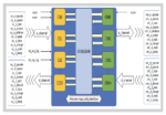
To fulfill the need for ever increasing bandwidth has put pressure to move faster to target bleeding edge technology nodes and to release faster new version of interconnect protocols (PCIe, Ethernet, memory controller). Innovation like PAM4 modulation and creation of DSP-based SerDes to replace old, 100% analog-based technique, were implemented, allowing to break the 100Gbps barrier. Innovative architecture has been defined pushing adoption of new standard like CXL, supporting cache-coherent memory sharing for processor, co-processor and AI accelerator, or Chip-to-Chip protocol between main SoC and chiplet, allowing to pass the technological area limit and offer more powerful system in a single package to support ever-increasing needs to compute and interconnect data flow, like in the year 2000 using a SoC has led to smartphone explosion.
If we synthetize, the next technology revolution will require using top interconnect and IP vendors will have to propose best-in-class interface IP, to create a successful IP business based on Stop-For-Top IP positioning. We think that offering Stop-For-Top IP should be the first step of a strategy, the final goal being to offer a chiplet portfolio, built by integrating already available interconnect IP into an Integrated Chip (IC), commonly named chiplet. To support this strategy, IP vendor will have to rely on a pool of dedicated resources specialized in ASIC design service. IP vendor will have to build this engineering team, whether organic or inorganic, by acquisition of an ASIC design service vendor.
Chip maker developing SoCs for high-end applications, such as HPC, datacenter, AI or networking are likely to be early adopters for chiplet architectures. Specific functions, like AI accelerators, Ethernet, PCIe or CXL standards should be the first interface candidate for chiplet designs. When these early adopters have demonstrated the validity of heterogeneous chiplet architecture, leveraging multiple different business models, and obviously the manufacturing feasibility for test and, packaging, it will create an ecosystem that is critical to support this new technology. At this point, we can expect a wider market adoption, not only for high-performance applications.
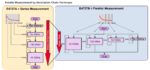
Like it was the case for Design IP sourcing to build a SoC in the 2000’s, the buy or make decision for chiplet sourcing to complete a system design, will be weighted between core competency protection and sourcing of non-differentiating functions. The historical and modern-day Design IP business growth since the 2000’s has been sustained by continuous increase of external sourcing. Both models will coexist (chiplet designed in-house or by a vendor) but history has shown that the buy decision eventually overtakes the make.
IPnest believes this trend will have two main effects in the interface IP business, one will be the strong growth of D2D IP revenues on the short term (2021-2025), and the other is the creation of the heterogenous chiplet market issued from Stop-For-Top IP portfolio. This market is expected to consist of complex protocols functions like PCIe, CXL or Ethernet. Even IP vendors delivering USB, HDMI, DP, MIPI interface IP integrated in SoCs I/O may decide to deliver I/O chiplet instead.
The Stop-For-Top IP model is the first step of a successful strategy followed by the creation of a chiplet portfolio by IP vendors to support industry need for open chiplet ecosystem. This ecosystem is needed by the semiconductor industry to overcome Moore’s Law limitation and reach the trillion dollars during the 2020 decade.
By Eric Esteve (PhD.) Analyst, Owner IPnest
This white paper has been sponsored by Alphawave IP, nevertheless the content reflects the author’s positioning about the IP market and the way it expected to evolve in the future, during the 2020 decade. To read the complete white paper:
Also read:
Die-to-Die IP enabling the path to the future of Chiplets Ecosystem
Design IP Sales Grew 19.4% in 2021, confirm 2016-2021 CAGR of 9.8%