Many years ago, I remember discussions around islands of automation/silos. Within the scope of any given silo there is plenty of automation to handle tasks relevant to that phase. But managing the full lifecycle from concept through manufacturing to field support must cross between silos, and those transitions are not as clean and automated. Over time more attention was paid to merging silos, through M&A and tighter integration, so now there are fewer but still bumpy and incompletely automated transitions.
Courtesy Siemens
The merging strategy will only take us so far. OEM system architecture, digital design, validation, manufacturing, and OEM product lifecycle management live in worlds which are too different to be pulled into one over-arching platform. Better connecting these phases in the lifecycle must rely on new interoperability standards and ideas. In the ideas department, Siemens proposes a concept of digital threads to interconnect data between silos.
What is a digital thread?
As Siemens puts it:
(Digital threads) collect, integrate, and manage data across the different stages of a product’s lifecycle. The goal is to then to harness that data in more advanced and interactive ways, which is achieved through a digital twin. While the digital thread provides a structured pathway of data across the lifecycle, the digital twin utilizes this data to dynamically mirror the real-world state, behavior, and performance of a particular product.
The digital twin is the engine to mirror the behaviors of a real-world capability (chip, car, factory), and digital threads are bi-directional data pathways weaving through the twin all the way from architecture to deployment. These act as a common source of truth between different product development and manufacturing/deployment phases, connecting both downstream and upstream, aiming to keep all phases through the lifecycle in sync with the most current expectations, assumptions, and implementation choices.
As described in their whitepaper, Siemens divides digital thread types into those originating or centered in architecture, components, design data, verification, and manufacturing/deployment. Remember that all these threads connect through the digital twin model (enabling shift-left design and optimization) and to the physical implementation (enabling cross correlation between the model and real-world prototype/deployment behavior).
The architecture, component, and design data threads
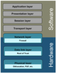
For me a perfect example (though not the only example) of the kind of data for which a thread makes sense in architecture is for traceability, a topic of great importance in automotive, aerospace and defense among other domains. Here the goal is to trace compliance with original OEM requirements, all the way through the lifecycle. And conversely to reflect unavoidable non-compliant changes made in design, so these become visible and actionable by all stakeholders through the lifecycle. Today much of this is accomplished through human review of natural language documents and spreadsheets. More sophisticated traceability systems aim for better mechanized compliance checking so that for example a requirement is matched to a design feature (with change notices if required) and to tests to validate compliance.
A second thread connects component data through the lifecycle. In component design, significant detail is generated for functional behavior, electrical, thermal, and other characteristics. After manufacturing, this data is heavily abstracted into PDF datasheets, losing almost all of the detail that an OEM might sometimes need to see, forcing information communication back to the stone age through human-only readable documents. System developers must craft their own databases to attempt (incompletely and inaccurately) to capture some of this detail from other documents and to add their own metrics such as cost and sourcing risk. Standards such as JEDEC JEP30 Part Model Guidelines aim to upgrade from this mess, to make a true component data thread possible. Another very important factor here is trust and (again) traceability for components. A digital thread can be signed, unlike the mess of documents on which we currently rely.
The design thread as I read it in this white paper primarily connects across the system implementation, from multi-die designs, PCB, module, and full electronic system, although I imagine similar value would extend to domain specific SoC design as a component in the overall system. This thread connects electronics, electrical and MCAD to provide a single source of truth for all requirements at this level, to guide design (including cabling), multiphysics analysis, EMC and even security. It also governs accessibility requirements so that sensitive data is available only to those who have been approved to have access to that data.
The verification and manufacturing/deployment threads
For the verification thread, emphasis in this white paper is on the system above the chip/chiplet level and on physical, parametrics and compliance. One example here is full system optimization based on AI methods, in sync with offerings from other vendors. The Siemens solution is called HyperLynx Design Space Exploration, which I’m guessing uses some form of automated Design of Experiments technique through covering arrays (I have talked about this elsewhere). The other important aspect of verification here is traceability, which I mentioned earlier. Mechanized traceability enables repeated and accurate checks against requirements derived directly from the original OEM requirements. This also enables checks to trigger automatically on a design checkin, facilitating continuous integration and deployment (CI/CD) for faster response time to changes.
For the manufacturing (and deployment) thread, the authors point out that while there are well-established standards and processes in support of handing off designs to manufacturing, there is no standardized feedback loop for issues discovered in manufacturing, such as product yield or component solderability. Nor is there a standardized mechanism to feed field discoveries back into the digital twin. We already know that reproducing post-silicon failures in a digital twin is much easier if a trace of circumstances leading up to the failure is available. Supporting post-manufacturing debug on a twin should be a priority at the board/system level as much as at the SoC level. Thinking further ahead, the paper also mentions growing importance of sustainability and recyclability; both concerns will inevitably reach back into earlier stages in the lifecycle chain.
Nice paper with much food for thought. You can access the paper HERE.