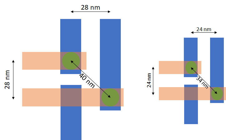


With metal interconnect pitches shrinking in advanced technology nodes, the center-to-center (C2C) separations between vias are also expected to shrink. For a 5/4nm node minimum metal pitch of 28 nm, we should expect vias separated by 40 nm (Figure 1a). Projecting to 3nm, a metal pitch of 24 nm should lead us to expect vias separated by 34 nm (Figure 1b).

Figure 1. (a) Left: 4nm 28 nm pitch M2 and M3 via connections may be expected to have center-to-center distance of 40 nm. (b) Right: 3nm 24 nm pitch M2 and M3 via connections may be expected to have center-to-center distance of 34 nm.
Is it really straightforward to do this by EUV?
Conventional EUV Patterning
A conventional EUV patterning would use a current 0.33NA EUV system to image spots smaller than 20 nm. However, for such an optical system, the spot is already limited to the image of the point spread function (PSF), which after resist absorption (e.g., 20%), has a highly stochastic cross-section profile (Figure 2).

Figure 2. Cross-section of point spread function in 20% absorbing resist. The stochastic characteristic is very apparent. The red dotted line indicates the classical non-stochastic image.
The real limitations from the point spread function from putting two of them together [1]. At close enough distances, the merging behavior is manifest by image slope reduction (degraded contrast) between the two spots (Figure 3). This is also accompanied by a change in the distance between the expected spot centers in the image, and stochastic printing between the two spots.

Figure 3. (a) Left: Absorbed photon number per sq. nm. for two point spread functions placed 36 nm apart. Note that the actual image C2C distance is 40 nm. (b) Right: Absorbed photon number per sq. nm. for two point spread functions placed 34 nm apart. The red dotted lines indicate the classical, non-stochastic images.
This means basically although two spots will appear, the chance of defects is too high to print them when running a high-throughput exposure. It would be safer to restrict them to be forbidden layout.
Alternative Patterning
Going to 0.55NA EUV worsens the stochastic behavior because of much lower resist absorption (e.g., 10%) due to the requirement for much thinner resist from severely limited depth of focus [2]. Such systems are also not available currently either, so the only remaining alternative is to print the two spots individually in separate exposures, i.e., double patterning [3]. Moreover, given that the EUV point spread function already has a significant stochastic distortion (see Figure 2), it would be better for a wider spot to be printed for each exposure (even by DUV) and post-litho shrink applied [4].
References
[1] F. Chen, Stochastic Behavior of the Point Spread Function in EUV Lithography, https://www.youtube.com/watch?v=2tgojJ0QrM8
[2] D. Xu et al., “Feasibility of logic metal scaling with 0.55NA EUV single patterning,” Proc. SPIE 12494, 124940M (2023).
[3] F. Chen, Lithography Resolution Limits: Paired Features, https://www.linkedin.com/pulse/lithography-resolution-limits-paired-features-frederick-chen/
[4] H. Yaegashi et al., “Enabled Scaling Capability with Self-aligned Multiple patterning process,” J. Photopolym. Sci. Tech. 27, 491 (2014), https://www.jstage.jst.go.jp/article/photopolymer/27/4/27_491/_pdf
This article originally appeared in LinkedIn Pulse: Application-Specific Lithography: Via Separation for 5nm and Beyond
Also Read:
NILS Enhancement with Higher Transmission Phase-Shift Masks
Assessing EUV Wafer Output: 2019-2022
Application-Specific Lithography: 28 nm Pitch Two-Dimensional Routing
Share this post via:


TSMC CoWoS versus Intel EMIB Semiconductor Packaging