If you want to know the state of play in lithography, there is no better place than the special session on lithography at Semicon West. This year was no exception. The session was given the punchy title Still a tale of 2 paths: multi-patterning lithography at 20nm and below: EUVL source and infrastructure progress.
In the blue corner for this fight were Stephen Renwick from Nikon (they make regular optical steppers) and Ben Rathsack of Tokyo Electron who is an expert on the rapidly-getting-less-esoteric technology called Directed Self Assembly (DSA). They represent the non-EUV side of things. In a second blog we’ll look at the red corner (or I suppose that should be violet corner) and what the EUV protagonists had to say.
Stephen talked about Argon Fluoride lithography extension (ArF) which for practical purposes is the only game in town for now. As he pointed out, you can still count the number of EUV tools worldwide on your fingers. ArF immersion is the lion’s share of the business but to further increase the resolution needs things like assisted pitch division, complementary lithography or more exotic solutions like DSA.
One interesting little fact is that it turns out that 90% of the masks are only used for 20% of the wafers. Or, to put it the other way around, 80% of all production is done using just 10% of the masks. Since CD uniformity is going down this is a challenge when boutique masks keep being thrown in.
Double patterning is cheaper than a slow EUV machine, and to date they are all slow (under 50 wafer per hour). True double patterning (self-aligned) can do spacer-based pitch halving and even pitch/6 and pitch/8. So ArF can deliver the required resolution for the forseeable future from a technology point of view.
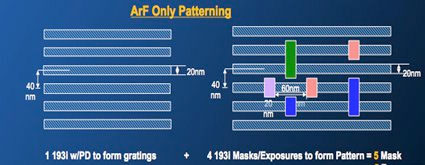
Complementary lithography is where we use pitch multiplication to lay down a grating of complete lines. Then using a cut mask split them up into the actual lengths required. Obviously this requires very restricted design rules but we already have a lot of that in 20nm and below anyway. The cut mask is the highest resolution (no pitch multiplication) but is also very sparse so technologies like e-beam or EUV might be applicable.
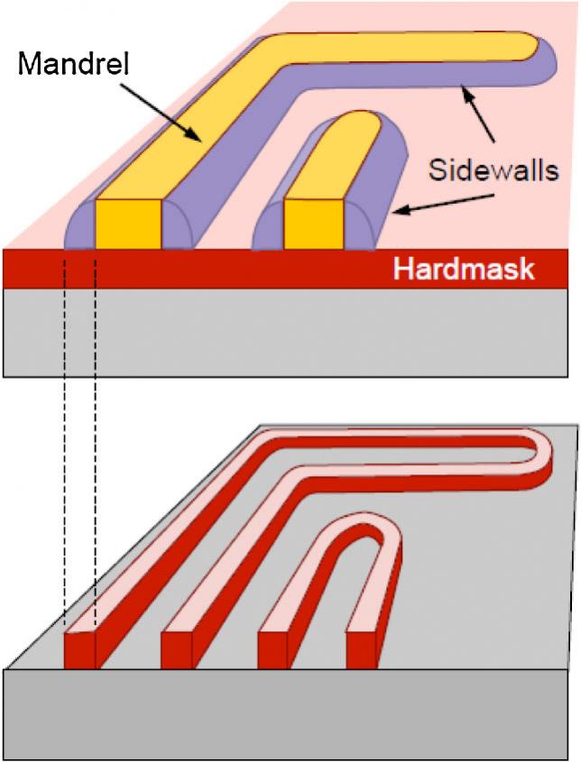
With pitch multiplication it turns out that resolution is not the limiting factor but overlay. Need about 2nm, today at 4nm but getting there. Machine-to-machine overlay is what counts (different steps in different steppers) already there for single machine overlay.
On the 450nm transition, Nikon intends to ship early learning tools based on 193 immersion for 450mm with shipments for production in 2017.
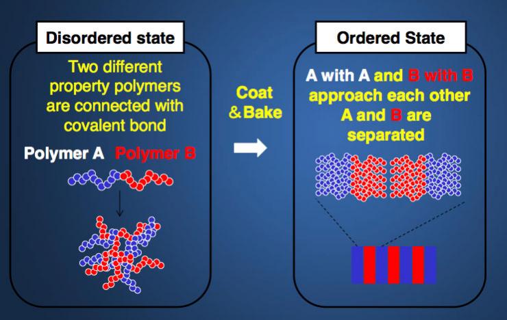 Ben Rathsack talked about building a collaborative ecosystem for DSA. DSA is so new that I’d better explain what it is. If you take two polymers with the right properties and join them with a covalent bond. Now if you bake them so they solidify then polymer A and polymer B separate themselves into separate areas. And if the polymers have the right property you can remove one of them and use the other as a mask for a process step. If you just pour this mixture on a wafer you just get a mess.
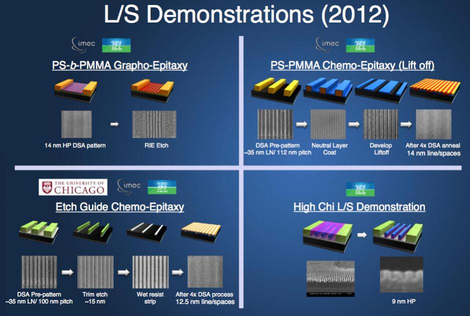
That is where the D in DSA, which stands for directed, comes in. If before you do this you lay down guide structures (using traditional 193i lithography) then the polymers will align nicely into a grating at a much finer pitch. Most of this work is still going on in academia, but is advancing rapidly.
Lines are good but you also need contacts/vias. Making small holes with self-healing approaches seems to work well too, but, as Ben pointed out “pitch pays the bills”. You need to be able to place the holes close together. Various approaches are being tried such as hole doubling (put the polymers into the right shaped rectangular slot and you get two circular vias) or making the vias in guide gratings so they form a line of contacts.
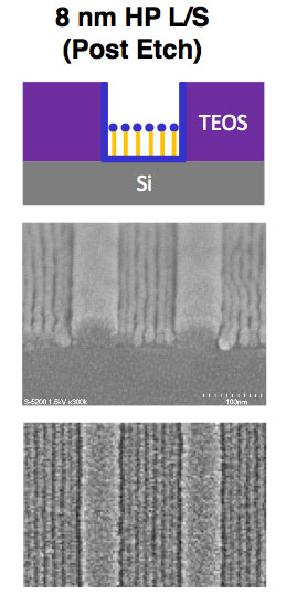 So DSA has advanced a lot since last year’s presentation. There is still a lot of work to be done to improve especially defect reduction, silicon fin integration (for FinFETs), sub-20nm holes, and also making it work with EUV eventually.
The really attractive things about DSA are:
- doesn’t require double, triple… patterning
- novel materials but existing process equipment
- many fewer process steps than quadruple patterning
- CD uniformity is entirely controlled by the polymer formation (1 step) whereas with multiple patterning many of the steps are very critical
Ben’s presentation is here. I’m not sure if you can access it if you didn’t attend Semicon or aren’t a SEMI member or don’t know the magic word. Unfortunately Stephen’s presentation doesn’t seem to be online.
Share this post via:


Comments
There are no comments yet.
You must register or log in to view/post comments.