







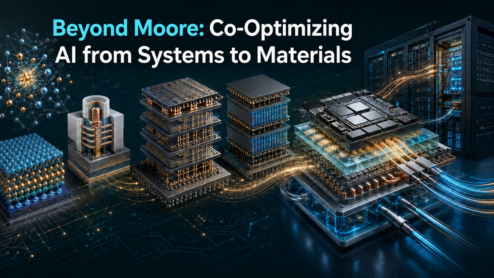
At the OCP APAC Summit in Taiwan, August 11–12, 2026, Applied Materials’ Subi Kengeri framed artificial intelligence as the semiconductor industry’s largest inflection point. AI demand is accelerating the industry toward one trillion dollars in annual revenue, but the keynote’s central message was more consequential than market growth: conventional node scaling alone cannot sustain the required improvement in compute. The next era will be constrained by energy, interconnects, packaging complexity and the speed at which the ecosystem can turn materials innovation into manufacturable systems.
The optimization dilemma is already visible. Scaling, advanced packaging and new architectures have reduced performance cost by roughly threefold across recent accelerator generations, while AI-server power consumption has also risen by about threefold. Capital expense is paid once; electricity and cooling costs continue throughout a system’s life. Energy-efficient performance, expressed through the interaction of capacitance, voltage, frequency and physical implementation, therefore becomes the decisive metric. The keynote set an ambitious target: a 10,000-fold improvement in energy-efficient performance by 2040.
Reaching that target requires simultaneous innovation across logic, memory and system integration. Gate-all-around transistors can deliver approximately 30% lower power and 15% higher performance, while backside power distribution can increase density by 30% and performance by 10%. High-bandwidth memory raises bandwidth by orders of magnitude, and vertical transistors and 3D DRAM promise further efficiency gains. Advanced packaging is the connective layer: the presentation projected up to 1,000 times higher I/O density and ten times lower energy per bit.
This transition makes heterogeneous integration the new frontier of scaling. A server processor from the 2000s might contain one die, about 100 square millimetres of silicon and a package complexity factor of one. A contemporary AI GPU can integrate 118 dies and reach a factor near 32,000. Future system-in-package designs may exceed 400 dies and a factor of 600,000. Such systems combine logic stacks, memory stacks, silicon or glass interposers, bridges, through-silicon or through-glass vias, embedded passives, redistribution layers and co-packaged optics.
Interconnect length directly affects bandwidth and power. Microbumps provide fewer than 1,000 I/Os per square millimetre at under 0.5 picojoules per bit. Hybrid bonding, by replacing longer solder-based connections with dense copper-to-copper interfaces, can scale from 10,000 toward one million I/Os per square millimetre while reducing energy below 0.05 picojoules per bit. The proposed future platform combines HBM hybrid bonding, 3.5D chiplet stacking, large interposers, bridges, passives, panel processing, glass substrates and optical connectivity.
Complexity at this scale cannot be solved by sequential device, package and system optimization. System Technology Co-optimization links micro-level process models, advanced-substrate models, package and system simulation, and die-boundary behavior. Electronic design automation is the engine: thermal, mechanical, signal-integrity and power effects must be solved concurrently. Co-packaged optics illustrates the need for an expanded process design kit, because assembly and packaging can represent more than half of process cost, and assembly, packaging and test together can exceed 80%.
For hyperscale operators, these advances alter the optimization boundary. Package architecture, cooling topology, power-delivery losses, repairability and workload placement must be evaluated together, not handed across organizational silos. Cost per transistor gives way to cost per useful function. Open interfaces are therefore essential: they allow chiplets from multiple suppliers to be qualified, combined and upgraded without surrendering system-level performance or reliability.
Bottom Line: The keynote concluded with an ecosystem agenda closely aligned with OCP. Industry needs workload-specific, modular chiplet architectures; rapid prototype vehicles that expose new failure mechanisms; design-for-test methods; interoperable data formats and interconnect protocols; clear supply-chain ownership; and known-functional-die standards. Applied Materials positioned its STCO platform, reusable chiplet prototype vehicle, participation in UCIe and OCP/OCE, and EPIC innovation center as mechanisms for collaboration. By connecting universities, suppliers, equipment makers, foundries, EDA providers and system companies, the proposed model aims to compress innovation cycles by twofold. The strategic conclusion is direct: leadership in AI will depend not merely on smaller transistors, but on co-optimizing materials, devices, packages, cooling, power delivery and software-visible architecture as one system.
Also Read:
Intel and TSMC Take Different Paths to High-NA EUV
Intel Foundry and the DAC2026 Ecosystem
The Difference Between TSMC CoWoS-S and CoWoS-R
Share this post via:



Terafab’s Single Roof: Why Packaging, Not Lithography, Decides High Volume