State-of-the-art chips will always include some portions which are memory arrays, which also happen to be the densest portions of the chip. Arrayed features are the main targets for lithography evaluation, as the feature pitch is well-defined, and is directly linked to the cost scaling (more features per wafer) from generation to generation. To that end, this article (second in the series on lithography resolution limits) focuses on the lithography resolution limits of arrayed feature patterning.
Minimum pitch resolution
A lithography tool is specified by the wavelength it uses, e.g., 193 nm for ArF, 13.5 nm for EUV, as well as its numerical aperture, i.e., the power of its final optic element (lens for ArF, KrF, i-line, mirror for EUV). The formula for the ideal minimum pitch between two lines in an array is
This result is derived from the grating equation [1]. Basically, the minimum pitch is realized by the interference of two beams which form the maximum angles with the optical axis, whose sines differ by wavelength/pitch. The difference of sines is at most equal to twice the numerical aperture – this gives the previously stated ideal minimum pitch. Realistically, though, the difference of sines must deduct the finite angular tolerance of the beams. The actual minimum pitch should therefore be
Hence, while for a wavelength of 193 nm, numerical aperture of 1.35, we ideally expect a minimum pitch of 71.5 nm, in reality it is 76 nm. Likewise for the EUV tool with nominal wavelength of 13.5 nm, numerical aperture of 0.33, the minimum pitch was recently demonstrated to be 24 nm [2], not the ideal 20.45 nm.
For two-dimensional arrays (square arrays, rectangular arrays, triangular arrays), the patterns can be generated by crossed line arrays, with best results achieved by using an attenuated (~5%) phase-shifting effect by the mask [3], so the same minimum pitch resolution limit, given by equation (2), applies as for lines.
In the previous article [4], it was noted that for a pair of features, the Rayleigh criterion (0.61 wavelength/numerical aperture) is used to determine the resolution. With arrayed features, although the pitch is already predetermined, the Rayleigh criterion applies if the array pitch is much wider than the distance set by that criterion; otherwise, it is the pitch (specifically, the half-pitch) that decides the resolution.
Self-aligned patterning: the ideal opportunity for arrayed features
When the minimum pitch needs to go below 0.5 wavelength/numerical aperture, a single exposure is not sufficient to pattern the array. A second exposure, such as the previously described LELE (litho-etch-litho-etch) approach [4], can achieve half the pitch, but alignment between the two exposures cannot be guaranteed. Self-aligned patterning approaches would be better. The most commonly practiced approach is Self-Aligned Double Patterning (SADP). Its earliest comprehensive description is given in US Patent 5328810, assigned to Micron after being filed in 1992 [5].
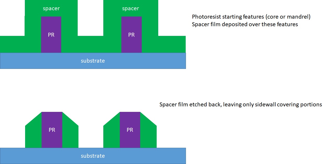
Figure 1 shows the first steps of basic SADP.
Figure 1. Basic SADP flow following standard lithography.
In this drawing, it is indicated clearly that the top of the spacer is eroded during the process. Also, it is the cost-reducing preference to use photoresist as the starting feature, rather than another etched material.
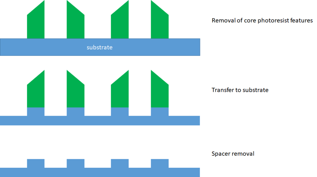
Figure 2 shows the completion of the SADP process.
 Figure 2. Completion of SADP process.
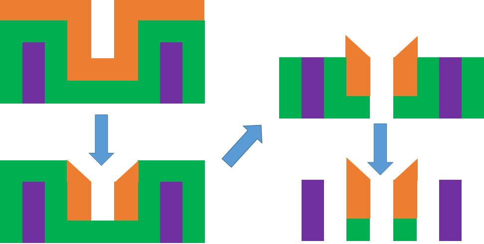
The new feature pitch on the substrate is now half the original photoresist feature pitch. Hence, this allows a doubling of line density, without an additional exposure. Sharp eyes may note that the distance between features in the center is a little wider than the distance between features where the photoresist was originally located. This effect is known as “pitch walking” [6]. This can arise from the original photoresist pattern, in combination with the spacer thickness, and the amount of spacer erosion. To manage the pitch walking the critical dimension (CD) of the starting photoresist feature must be in sync with the spacer thickness and erosion rate. Alternatively, a gapfill material may be deposited after the spacer film is deposited [5,7].
This protects the exposed spacer side from erosion, but leaves extra spacer material to be removed later along with the gapfill material, as well as the starting core feature. This can be extended, however, to more than doubling feature density. For example, Samsung’s US Patent 7842601 [8] describes the double spacer approach to reducing line pitch to one-third its original value (Figure 3). This allows a 78 nm pitch (~22nm foundry node design rule) to be immediately reduced to 26 nm (<5nm foundry node design rule) in a single exposure, without using EUV.
Figure 3. Self-aligned triple patterning (SATP) by the use of two spacers.Two-dimensional self-aligned patterning
When the SADP process is applied to two-dimensional patterns, the possibilities expand. For example, in Figure 4, features on a square lattice are doubled in density.
 Figure 4. Two-dimensional SADP on a square lattice doubles feature density.
The central added feature is expected to round out like the original corner features of the lattice cell. Going even further, a triangular or hexagonal lattice allows feature density to be tripled.
Figure 5. Two-dimensional SATP on a triangular lattice triples feature density.
The latter approach has already been used in Samsung’s 20nm DRAM [9] for the honeycomb capacitor patterning.
Double SADP/SATP in 2D?
By repeating the SADP/SATP processes described above, the arrayed feature density increases in leaps and bounds. Double SADP quadruples density for line arrays and square lattices; hence, this is also referred to as self-aligned quadruple patterning (SAQP). Double SATP in two dimensions noncuples (multiplies 9x) density for triangular lattices.
The feasibility of double SADP is tied to the process complexity. The complexity of double SADP is increased over that of single SADP, but having several consecutive etch steps which can be executed at the same etch station is easier to manage. The etch rates of three materials (core, spacer, substrate) are considered simultaneously in any case. On the other hand, a new EUV resist process flow may involve added deposition and treatment steps inserted (Figure 6). In particular, the new underlayer material being etched could have its own station, as it may be organic [10] or metal-based [11]. The underlayer benefit is expected from the effects of secondary electrons released by EUV light [12].
Share this post via:


The Intel Common Platform Foundry Alliance