What is FMS?
Our over-arching mission is to help accelerate the move towards a world where advanced memory and storage technologies enable AI systems, data centers, hyperscalers and enterprises to operate at unprecedented scale, speed and efficiency. All the while supporting the engineers and architects building the infrastructure… Read More
The 18th IEEE International Memory Workshop (IEEE IMW) will be held in 2026 in Leuven, Belgium. It is currently planned as an on-site event. This conference brings the memory community together in a workshop environment to discuss the memory process and design technologies, applications, market needs and strategies. It is sponsored… Read More
The explosive growth of AI and accelerated computing is placing unprecedented demands on system-on-chip (SoC) design. Modern AI workloads require extremely high bandwidth, ultra-low latency, and energy-efficient data movement across increasingly heterogeneous architectures. As SoCs scale to incorporate clusters of… Read More
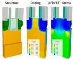
Semiconductor fabs aim to have high yields and provide processes that attract design firms and win new design starts, but how does a fab deliver their process nodes in a timely manner without having to run lots of expensive silicon through the line? This is where simulation and TCAD tools come into play, and to learn more about this… Read More
A recent TechSpot article suggests that Apple is moving cautiously towards release of some kind of generative AI, possibly with iOS 18 and A17 Pro. This is interesting not just for Apple users like me but also for broader validation of a real mobile opportunity for generative AI. Which honestly had not seemed like a given, for multiple… Read More
-Lam reported in line results on reduced expectations
-Guidance disappoints as memory decline continues
-Memory capex down 50% but still sees “further declines”
-Lam ties future to EUV maybe not good idea after ASML report
Lam comes in above grossly already reduced expectations
and misses on guidance
We always … Read More
State-of-the-art chips will always include some portions which are memory arrays, which also happen to be the densest portions of the chip. Arrayed features are the main targets for lithography evaluation, as the feature pitch is well-defined, and is directly linked to the cost scaling (more features per wafer) from generation… Read More
For decades development work on Artificial Intelligence (AI) and Machine Learning (ML) was done on traditional CPUs and memory configurations. Now that we are in the “hockey stick” upturn in deployment of AI and ML, the search is on for the most efficient types of processing architectures. The result is a wave of development for… Read More
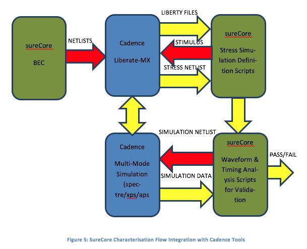
If you are designing an SOC for an IoT application and looking to minimize power consumption, there are a lot of choices. However, more often than not, looking at reducing SRAM power is a good place to start. SRAMs can consume up to 70% of an IC’s power. SureCore, a leading memory IP supplier, offers highly optimized SRAM instances … Read More