The most powerful approach to managing the complexity of current SoC hardware is the identification of hierarchical instances with which to assemble the design. The development of the hierarchical design representation requires judicious assessment of the component definitions. The goals for clock distribution, power management, and circuit/routing utilization require partitioning that is neither too fine nor too coarse – e.g., the management of multiple power domains within a large partition is difficult, while too fine a partitioning results in more pin constraints to manage and fewer opportunities for timing-driven physical design optimizations.
It struck me that the tradeoffs to the hierarchical representation directly apply to the architecture of an FPGA, as well. I recently chatted with Cheng Wang, SVP of Engineering at Flex Logix Technologies, about how they approached the hierarchical decomposition of the design complexity of their embedded FPGA cores – it was an extremely enlightening discussion.
First, I needed to study up on the typical hierarchical architecture of an FPGA. The programmable logic is implemented with n-input look-up tables (LUT’s). A logic block consists of multiple LUT’s, with additional storage bits. Dedicated local routing connects the LUT’s within the block. The traditional FPGA uses an island style architecture, with logic blocks separated by wiring channels. (This architecture is also denoted as a “mesh” style design.)
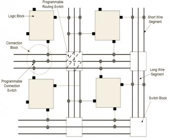
Figure 1. General FPGA island architecture. (From: Rose and Betz, “How Much Logic Should Go in an FPGA Logic Block?”, IEEE D&T of Computers, January 1998.)
The input and output signals of logic blocks are connected to segmented wires in the channels. The logic block-to-channel wire assignment is denoted as the “connection box”. The pins of the logic block are connected to a percentage of the wires in the channel (Fc), typically between 50% and 100% of the channel track width.
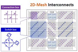
Figure 2. Expanded view of the connection box and switch box of an FPGA mesh architecture. (From: D. Markovic, “FPGA Architecture”, UCLA EE216B.)
The figure above depicts “un-segmented” channel wires and pass transistors for logic block connections. Alternatively, wire segments are commonly used – the figure below illustrates a block input pin connected to three segments, with the active segment using a buffer + MUX shown in red.)
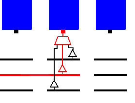
Figure 3. Segmented wires in the channel connected to a logic block input. (From: V. Betz, “FPGA Architecture”, University of Toronto).
The channel wires are connected to programmable switches, located in the “Switch Box”. The Switch Box design defines how channel wires may connect to wires on other sides – the “flexibility” of the switch box is a parameter that indicates how many other wires are potential connections.
Note in the figures above that clock wires are not shown – the common approach is to include specific global and local wiring tracks for clocks to the logic block storage elements. The dedicated clocks include distributed buffering and clock management units.
FPGA architecture design involves balancing multiple tradeoffs related to the implementation hierarchy:
- Logic block functionality needs to address performance, utilization, and routability. A fine-grained block design will require more programmable interconnect resources, more switches, and correspondingly, less performance. A very rich (coarse-grained) logic block design will be inefficient for small logic functions. The goal is to find an optimum logic block functionality, which aligns with the capabilities of the logic synthesis and physical design tools. FPGA implementations have commonly ranged from 4-10 LUT’s connected locally in the logic block. As FPGA synthesis has improved, the common LUT design has also evolved, from 4- to 5- to 6-input (with dual 5-input) functionality, as is the case for the current Flex Logix EFLX architecture.
- FPGA design has also evolved to include special-purpose blocks. The hierarchical implementation needs to be able to readily support the unique programmable logic design of arithmetic and DSP functions.
- The FPGA routing architecture needs to provide sufficient resources to satisfy both utilization and performance targets.
With that background, I asked Cheng, “How did Flex Logix approach these implementation hierarchy decisions?”
He answered, “Rather than the island architecture, we adopted a hierarchical switch network. The number of switch connections required for routes with high locality is reduced, improving performance.”
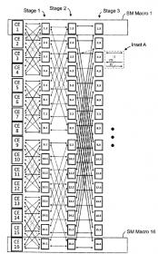
Figure 4. Hierarchical switch network for FPGA connectivity. (From: US Patent 9,503,092.)
“Of specific importance is the radix and depth of the hierarchical network tree, which were chosen to optimize the overall routability – the top level of the switch network utilizes the mesh routing of the island architecture.”, Cheng continued.
“What other hierarchical tradeoffs were faced?”, I asked.
Cheng replied, “We recognized two key design goals for embedded FPGA IP. For many applications, customers need to implement power gating on some of their eFPGA functionality. And, for performance, customers require optimal, low-skew clock distribution, with support for integrating multiple clock domains. To meet these requirements, we introduced a hierarchical component denoted as a tile.”
The Flex Logix hierarchical tile functionality includes ~2,500 6-input, 2-output LUT’s (16nm), with two optional flops per LUT.
Cheng highlighted, “Within a tile, the programmable logic can be power gated for a low-power application. The tile design includes an optimized H-tree clock, supporting either one or two clock domains. We implemented a novel method for balanced H-tree construction to distribute a clock input across multiple tiles.”
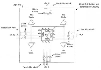
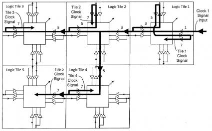
Figure 5. Clock distribution within and between tiles, for balanced H-tree distribution. A clock may enter a tile at any edge, with multiplexing to distribute through a consistent number of buffers throughout multiple tiles. (From: US Patent 9,882,568.)
“With the introduction of the hierarchical switch network and the tile hierarchy for clock and power management, we needed to develop our own netlist placement and routing technology. These algorithms provide improved performance, with a reduced number of switches for logic localized to the lower levels of the hierarchical network.”, Cheng said.
The design of eFPGA IP requires supporting a range of end-customer logic capacities with aggressive utilization and performance targets, while supporting varied clock and power domain designs. The introduction of the hierarchical “tile” achieves these goals.
The next time we get together for coffee, Cheng is going to share how the tile boundary design enables efficient signal communication between adjacent tiles – it should be an interesting discussion.
For more information on these eFPGA hierarchical implementation design options, please follow this link.
-chipguy
Read more about Flex Logix on SemiWiki


Comments
There are no comments yet.
You must register or log in to view/post comments.