In this era of high-performance, low-power, and low-cost devices coming up at an unprecedented scale, the SoCs can never attain the ultimate in performance; always there is scope for improvement. Several methods including innovative technology, multi-processor architecture, memory, data traffic management for low latency, and software have been explored with great success in enhancing SoC performance. However, the bottleneck of memory access for high-speed processing has always been an issue.While the memory interface speed has increased significantly, the core memory speed has lagged behind. This is why the concept of pre-fetching more words in a single cycle came and DDR2, DDR3, DDR4, and several of their other variants evolved.
Along with increasing memory access speed come several challenges such as signal integrity, priority queuing, bandwidth utilization, memory allocation and management, and so on. The memory interface IP must provide a complete robust solution for high-speed memory access. As I mentioned in one of my whitepapers on IP cost considerations, it’s time for IP providers to include a complete solution in their IP to add value and enable differentiation.
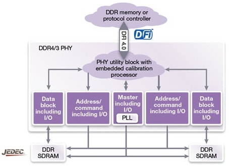
Synopsys Designware[SUP]®[/SUP]DDR4/3 PHY IPprovides a complete solution for SoCs to integrate high-performance DDR4/DDR3/DDR3L SDRAM interfaces operating at up to 3200 Mbps speed. The IP includes a first-of-its-kind Embedded ARC[SUP]®[/SUP]Calibration Processor to execute PHY independent, hardware-assisted, firmware-based training algorithms for effective memory management.

The DDR4/3 PHY IP is primarily delivered as GDSII including integrated application-specific DDR4/3 I/Os. It includes a low-jitter PLL for clock generation for both PHY and SDRAM. The IP includes a DFI 4.0 interface that can connect to any internal controller, or Synopsys’ Enhanced Universal Memory controller (uMCTL2) or Protocol controller (uPCTL2) for a complete and flexible DDR interface solution.
The PHY utility block (PUB), containing the Embedded Calibration Processor is RTL-based and provides control for important operations including read/write leveling, per bit data deskew, and data eye training through voltage and temperature compensated delay lines. It also supports production testing for the PHY. The VT compensated delay lines are used for centering the clock in the address and command windows.
The DDR4/3 PHY includes a host of features making it versatile enough to provide wide ranging solutions for high-speed memory interfaces. It supports up to 16 logical ranks for high capacity memory requirements with 8 to 72 bit data path widths; providing up to a maximum of 230 Gbps bandwidth for a 72-bit wide data bus. To ensure robust operation at such high data rates, a signal integrity report can be provided which can be analyzed to identify issues and take corrective action during the design reviews.
The I/Os include receiver decision feedback equalization (DFE) and driver feed-forward equalization (FFE). The IP supports up to 4 trained states/frequencies with <5us switching time and each state maintained across voltage and temperature variation. There are inactive idle states for power saving – ‘DFI_LP Mode’ where most clocks and delay lines are gated; ‘PHY Inactive’ for leakage only; ‘PHY Retention’ where core power is removed, most I/Os are powered down, and SDRAMs are held in self-refresh mode.
The DDR4/3 PHY IP supports JEDEC standard DDR4, DDR3, and DDR3L SDRAMs and is compatible with JEDEC compliant DDR3/4 UDIMMs and RDIMMs as well as DDR4 LRDIMMs. This is ideal for high-performance, high-capacity memory solutions required for servers, PCs, and even for tablets and mobile products.
Synopsys provides DDR4/3 PHY IP at 28-nm, 16-nm, 14-nm, and lower technology nodes. It’s apparent that the IP provider incurs considerable cost to provide the IP at multiple nodes. With DDR4 IP at faster process nodes, fewer pipeline stages, and some changes in functionality, Synopsys has achieved significantly lower latency compared to DDR3.
There are many features which are specific to DDR4 and provide superior solutions for memory interfaces. Read the DesignWare DDR4/3 PHY IP datasheet at Synopsys’ website HERE for a complete list of DDR4/3, DDR4 exclusive, and I/O features.
Pawan Kumar Fangaria
Founder & President at www.fangarias.com


Comments
There are no comments yet.
You must register or log in to view/post comments.