







As wireless communication systems evolve toward 6G, satellite connectivity, advanced radar, and high-performance sensing applications, the integration of heterogeneous semiconductor technologies has become a critical challenge. Silicon CMOS remains the dominant platform for digital processing and system control, while III-V semiconductor materials such as GaN, InP, and GaAs continue to provide superior high-frequency and high-power performance. Bridging these technologies into a single package has emerged as a key enabler for next-generation RF and mixed-signal systems.
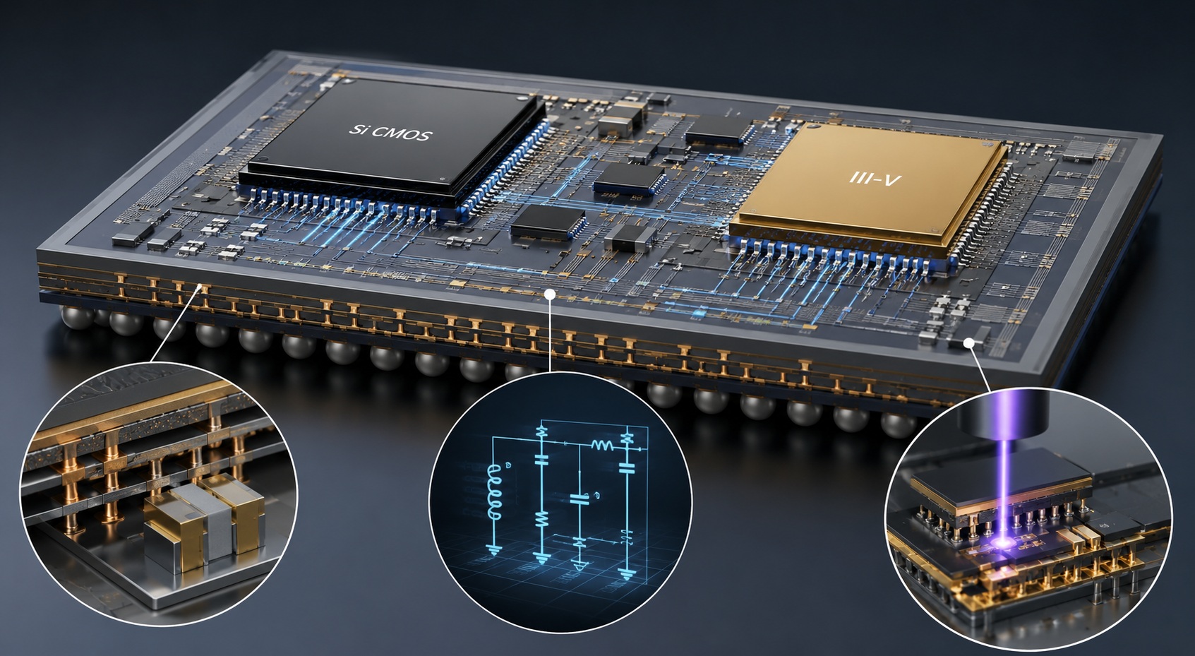
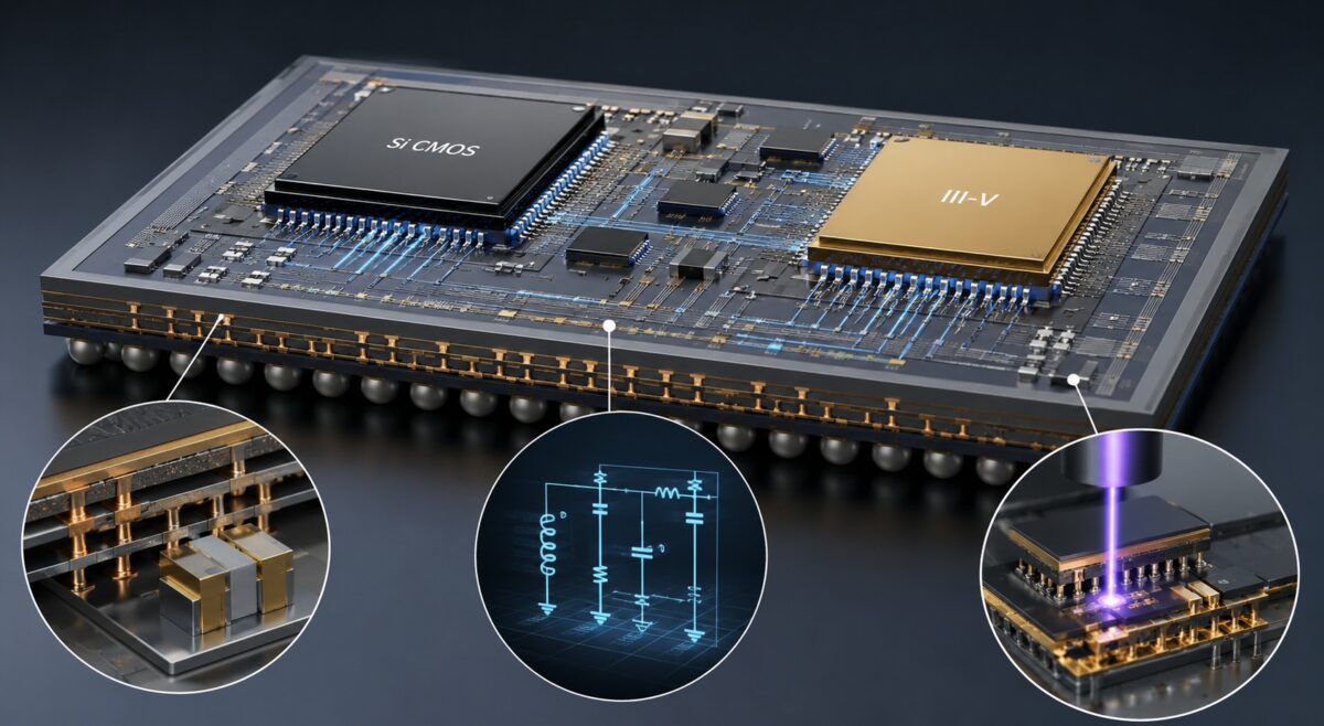
Researchers at imec have demonstrated significant progress toward this goal by advancing their 300mm RF silicon interposer platform. The latest developments combine high-density metal-insulator-metal capacitors (MIMCAPs), comprehensive passive-device modeling, and laser-assisted chiplet bonding technologies, creating a scalable pathway for system-level integration of III-V chiplets with silicon CMOS infrastructure.
The foundation of the platform is a silicon-based RF interposer manufactured on 300mm wafers using CMOS-compatible processes. Unlike conventional packaging substrates, the interposer functions as an active integration layer, providing high-density routing, impedance-controlled interconnects, and embedded passive components. This approach enables designers to partition complex systems into optimized chiplets, allowing each function to be fabricated using the most appropriate semiconductor technology while maintaining high electrical performance.
A key enhancement to the platform is the integration of high-density MIM capacitors. These embedded passives provide localized energy storage, RF filtering, impedance matching, and signal conditioning without consuming valuable chip area on the active die. By integrating MIMCAPs directly within the interposer stack, system designers can reduce parasitic inductance, improve power integrity, and achieve more compact RF front-end architectures. The high capacitance density also supports advanced millimeter-wave and sub-THz circuit implementations where passive component performance directly impacts overall system efficiency.
To maximize the value of embedded passives, imec has developed accurate electromagnetic and circuit-level models for interposer-integrated passive structures. These models encompass capacitors, transmission lines, inductors, and complex routing networks, enabling precise prediction of RF behavior across a broad frequency spectrum. The resulting design framework allows engineers to perform co-optimization of chiplets, package interconnects, and passive components during the earliest stages of development. Such predictive capability is essential for emerging applications operating above 100 GHz, where parasitic effects can significantly influence gain, noise figure, linearity, and power efficiency.
Another major innovation is the implementation of laser-assisted bonding technology for heterogeneous chiplet assembly. Traditional thermal bonding approaches often expose devices to elevated temperatures that can introduce mechanical stress, material degradation, or alignment challenges. Laser-assisted bonding delivers localized energy precisely at the bonding interface, enabling strong electrical and mechanical connections while minimizing thermal impact on surrounding structures.
This capability is particularly valuable for integrating III-V devices onto silicon interposers. Materials such as gallium nitride and indium phosphide possess thermal expansion characteristics that differ significantly from silicon. Localized laser processing reduces thermomechanical stress and facilitates high-yield attachment of diverse chiplet types. The technique also supports fine-pitch interconnect formation, which is essential for achieving the bandwidth and signal integrity requirements of advanced RF systems.
The combination of embedded MIMCAPs, accurate passive modeling, and laser-assisted bonding transforms the RF interposer from a packaging substrate into a high-performance system integration platform. Designers can combine CMOS digital processing, III-V RF power amplifiers, low-noise amplifiers, photonic devices, and advanced sensors within a unified architecture while preserving the performance advantages of each technology node.
Bottom line: For future wireless infrastructure, satellite communications, automotive radar, and sensing systems, this heterogeneous integration strategy offers a practical route to overcoming the limitations of monolithic scaling. By leveraging mature 300mm manufacturing infrastructure and advanced chiplet assembly techniques, imec is demonstrating how silicon interposers can serve as the backbone for next-generation heterogeneous systems, enabling unprecedented levels of performance, functionality, and design flexibility across the semiconductor ecosystem.
For more information, visit www.imec-int.com
Also Read:
Feed Forward Intelligence: Enabling Testability in the Chiplets Era
Technical Paper: FPGA Prototyping That Creates Useful PreSilicon Evidence
Share this post via:



SEMICON West’s Autonomous Fab Vision Needs a Decision-Escalation Design