

Synopsys has announced the availability of the first wave of its Multiphysics Fusion Solutions, extending its vision of a unified engineering environment that connects EDA, semiconductor physics, system simulation, and artificial intelligence-driven optimization. The announcement addresses one of the most significant challenges facing advanced semiconductor and system design: accurately modeling the interaction of electrical, thermal, mechanical, optical, and electromagnetic effects across increasingly complex products.
As semiconductor technologies advance into the angstrom era and heterogeneous integration becomes mainstream, traditional design methodologies are reaching their limits. Modern chips are no longer isolated electronic devices. They operate within highly integrated systems that include advanced packaging, chiplets, high-bandwidth memory, photonics, power delivery networks, and complex cooling infrastructures. These systems exhibit tightly coupled multiphysics behavior that can directly impact performance, reliability, power consumption, and time-to-market.
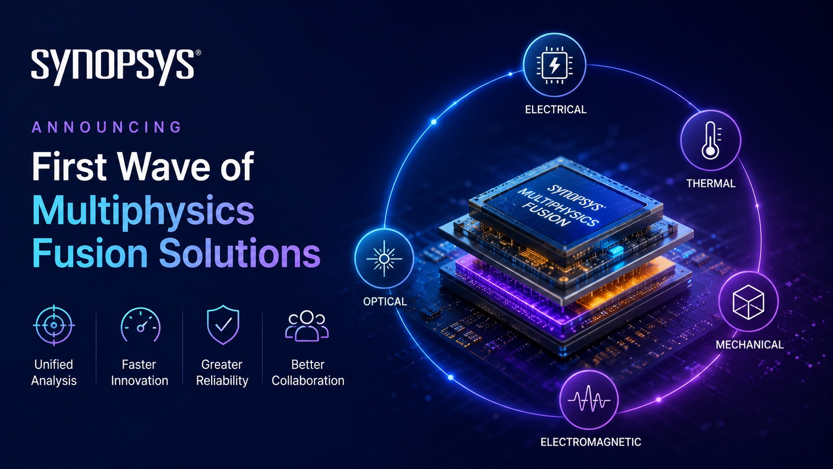
The Synopsys Multiphysics Fusion Solutions portfolio is designed to provide a unified digital twin environment where engineers can analyze and optimize multiple physical domains simultaneously. Rather than performing separate simulations for electrical, thermal, mechanical, and electromagnetic effects, the Fusion platform enables concurrent analysis with shared data models and interoperable workflows.
At the heart of the approach is the integration of traditionally separate simulation technologies into a common framework. Electrical simulation can be directly correlated with thermal analysis to identify hotspots that affect transistor performance. Mechanical stress modeling can be linked to package reliability studies. Electromagnetic simulations can be combined with signal integrity and power integrity analysis to identify potential issues before fabrication.
The need for this capability is becoming increasingly urgent as advanced packaging technologies such as 2.5D and 3D integrated circuits gain widespread adoption. Through-silicon vias (TSVs), silicon interposers, and stacked-die architectures create new interactions between heat, power delivery, and mechanical stress. A thermal hotspot in one die can affect the performance and reliability of neighboring dies, while package warpage can influence electrical connectivity and long-term reliability.
Synopsys is also leveraging artificial intelligence to accelerate multiphysics analysis. AI-assisted optimization can rapidly explore design tradeoffs across multiple domains, helping engineers identify optimal solutions that balance performance, power, area, cost, and reliability. This capability is especially valuable as simulation workloads continue to grow exponentially with design complexity.
Another important aspect of the Multiphysics Fusion strategy is the creation of a consistent digital thread across the semiconductor development process. Data generated during device design, package development, board implementation, and system validation can be shared more effectively, reducing the need for manual data translation and minimizing opportunities for errors. This unified approach improves collaboration among traditionally siloed engineering teams.
The first wave of Fusion solutions targets several critical applications, including advanced packaging, multi-die systems, photonics, thermal management, and reliability analysis. These areas are among the fastest-growing segments of the semiconductor industry and represent key enablers for artificial intelligence infrastructure, high-performance computing, automotive electronics, aerospace systems, and next-generation communications platforms.
Why It Matters
The significance of Synopsys’ Multiphysics Fusion Solutions extends beyond simulation efficiency. The semiconductor industry is entering an era where system-level interactions often determine product success more than transistor-level scaling alone. As Moore’s Law slows and system complexity increases, innovation increasingly comes from integration, packaging, and heterogeneous architectures.
Traditional point tools cannot adequately capture the coupled physical effects that drive performance and reliability in these systems. Engineering teams need a holistic view of how electrical, thermal, mechanical, and optical phenomena interact throughout the design lifecycle. The ability to identify issues early in development can prevent costly redesigns, improve yield, accelerate qualification, and reduce overall development risk.
Bottom line: For AI data centers, advanced automotive systems, and high-performance computing applications, thermal and power challenges are becoming primary design constraints. Multiphysics simulation provides the insight needed to optimize these systems before silicon is manufactured. As a result, Synopsys’ Fusion strategy represents an important step toward the industry’s broader transition from isolated design tools to comprehensive digital engineering platforms that enable faster innovation and more predictable product outcomes.
Also Read:
Customized Foundation IP Enables the Next Generation of Automotive Compute
Intel: Pushing EMIB Forward: Design Methodology Insights with Synopsys Tools
Share this post via:


Comments
There are no comments yet.
You must register or log in to view/post comments.