You are currently viewing SemiWiki as a guest which gives you limited access to the site. To view blog comments and experience other SemiWiki features you must be a registered member. Registration is fast, simple, and absolutely free so please,
join our community today!
The central argument of Ankur Gupta’s AI Infra Summit keynote is simple but consequential: the next leap in AI infrastructure will not come from improving chips, servers, cooling systems, or data centers independently. It will come from optimizing the connections among them. Siemens frames this as a journey “from custom silicon… Read More
The reported move of Amit Gupta, Jeff Dyck, and Ryan Silk from Siemens EDA to Synopsys matters because this is more than a routine transfer of experienced executives and engineers. Together, the three represent a concentrated body of expertise in applying artificial intelligence to semiconductor design—one of the most strategically… Read More
Signoff-quality design tools are mandatory for signoff, though not so good for early design exploration. Signoff demands high accuracy in design description and high precision in analysis. The first requirement can’t be met early in design where architecture decisions are still in flux, and the second depends on very detailed… Read More
NVIDIA’s expansion of the NVIDIA Agent Toolkit with PhysicsNeMo and CUDA-X libraries marks a shift from general-purpose AI assistants toward autonomous engineering systems. Instead of limiting agents to document retrieval, code generation, or workflow automation, the expanded toolkit lets developers connect reasoning… Read More
What systems can accomplish by combining semiconductors, AI, and software seems at times boundless. Chiplet-based semiconductors deliver this promise, allowing a myriad of complex digital, memory, analog and photonic functions to be condensed into a single semiconductor package for higher performance, lower power consumption… Read More
Synopsys has announced the availability of the first wave of its Multiphysics Fusion Solutions, extending its vision of a unified engineering environment that connects EDA, semiconductor physics, system simulation, and artificial intelligence-driven optimization. The announcement addresses one of the most significant… Read More
The semiconductor industry is rapidly moving beyond traditional 2D packaging, embracing technologies such as 3D integrated circuits (3D ICs) and 2.5D advanced packaging. These approaches combine heterogeneous chiplets, silicon interposers, and complex multi-layer routing to achieve higher performance and integration.… Read More
In a major announcement at the 2025 Design Automation Conference (DAC), Siemens EDA introduced a significant expansion to its electronic design automation (EDA) portfolio, aimed at transforming how engineers design, validate, and manage the complexity of next-generation three-dimensional integrated circuits (3D ICs).… Read More
At NVIDIA’s recent GTC conference, a Cadence-NVIDIA joint session provided insights into how AI-powered innovation is reshaping the future of data center infrastructure. Led by Kourosh Nemati, Senior Data Center Cooling and Infrastructure Engineer from NVIDIA and Sherman Ikemoto, Sales Development Group Director from … Read More
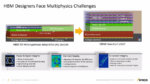
3D design with high-bandwidth memory stacks (HBM) has become essential for leading edge semiconductor systems in multiple applications. Hyperscalers depend on large AI accelerator cores supported by 100GB or more of in-package HBM to handle trillion parameter AI models. Autonomous Drive (AD) vehicles may handle smaller … Read More