The final session of the SEMI Industry Strategy Symposium (The CxO Panel) was the most interesting for me because executives from three of the four most influential semiconductor companies were on the panel: Dr. Goeff Yeap of Qualcomm, Dr. Jack Sun from TSMC, and Mr. Mark Bohr of Intel. Who is fourth you ask? That would be Apple of … Read More

ANSYS Updates RedHawk for FinFET Nodes

Most designers are not using FinFETs yet, however the increased transistor density and power advantages they offer are compelling. Smaller feature sizes have been a consistent driver in semiconductor technology. Eventually the market will move more and more to FinFET processes, increasingly leaving behind planar transistors.… Read More
Who is REALLY Using TSMC 16FF+?
As I wrote last week there is a whole list of companies on LinkedIn with people working on TSMC 16nm. Today TSMC released a list of customers that have risk production 16FF+ silicon. Most of us knew this already but now we can talk about it in more detail. This is a really big deal for the FinFET doubters out there. Just because Intel had… Read More
Let the FinFET Yield Controversy Begin!
It never ceases to amaze me how people point fingers and create controversy to cover their mistakes. It happened at 40nm, 28nm, and again at 20nm and now it is time for the regularly scheduled yield controversy. Of course any conversation about semiconductor yield generates clicks for SemiWiki so I’m happy to play along.
It generally… Read More
Noise & Reliability of FinFET Designs – Success Stories!
I think by now there has been good level of discussion on FinFET technology at sub-20 nm process nodes and this is an answer to ultra dense, high performance, low power, and billion+ gate SoC designs within the same area. However, it comes with some of the key challenges with respect to power, noise and reliability of the design. A FinFET… Read More
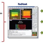
ANSYS Tools Shine at FinFET Nodes!
In the modern semiconductor ecosystem we are seeing rapid advancement in technology breaking past once perceived limits; 28nm, 20nm, 16-14nm, 10nm and we are foreseeing 7nm now. Double and multi-patterning are already being seen along with complex FinFET structures in transistors to gain the ultimate advantages in PPA from… Read More
Place & Route with FinFETs and Double Patterning
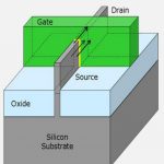
Place & route in the 16/14nm era requires a new approach since it is significantly more complex. Of course, every process generation is more complex than the one before and the designs are bigger. But modern processes have new problems. The two biggest changes are FinFETs and double patterning.
FinFETs, as I assume you know,… Read More
Samsung 14nm FinFET Design with Cadence Tools
The first consumer products with 20nm processing are arriving in 2014 like the 2 billion transistor A8 chip in the iPhone 6, however at the 14nm node there are new designs underway to continue the trend of Moore’s Law. To get a better feel for the challenges of designing with 14nm FinFET technology I watched a 23 minute video … Read More
FinFET Design for Power, Noise and Reliability

IC designers have been running analysis tools for power, noise and reliability for many years now, so what is new when you start using FinFET transistors instead of planar transistors? Calvin Chow from ANSYS (Apache Design) presented on this topic earlier in the summer through a 33 minutewebinar that has been archived. There is… Read More
FinFETs for your Next SoC
Planar CMOS processes have been offered for decades now, and all the way down through the 28nm node it has been riding the benefits of Moore’s Law. A few years back we started hearing from Intel about TriGate (aka FinFET) starting at the 22nm node as a way to use a more 3D processing approach for transistors instead of planar CMOS.… Read More
TSMC CoWoS versus Intel EMIB Semiconductor Packaging