You are currently viewing SemiWiki as a guest which gives you limited access to the site. To view blog comments and experience other SemiWiki features you must be a registered member. Registration is fast, simple, and absolutely free so please,
join our community today!
WP_Term Object
(
    [term_id] => 89
    [name] => FinFET
    [slug] => finfet
    [term_group] => 0
    [term_taxonomy_id] => 89
    [taxonomy] => category
    [description] =>
    [parent] => 0
    [count] => 233
    [filter] => raw
    [cat_ID] => 89
    [category_count] => 233
    [category_description] =>
    [cat_name] => FinFET
    [category_nicename] => finfet
    [category_parent] => 0
    [is_post] =>
)
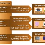
We live in very interesting times, you can wear an Android watch from Samsung that uses 14 nm FinFET technology, attend the 52nd DAC conference in June to learn about EDA and IP vendors supporting FinFET, and read about research work for new devices down to 5 nm. TCAD is that critical software technology that enables the development… Read More
At the TSMC Technology Symposium last month Suk Lee presented a lot of information on design enablement. Suk is an interesting guy with a unique background in ASIC, Semiconductor, EDA, and now Foundry. In baseball terms that would be like playing infield, outfield, home plate, and umpire!
Around the turn of the millennium Suk actually… Read More
There was an article on Motley Fool recently detailing Intel’s 14nm FinFETs and comparing them to TSMC. Unfortunately the author has zero semiconductor education or experience even though he writes with authority on all things semiconductor. He also has no shame in using outdated papers from conferences he did not even… Read More
As a professional conference goer I can see definite trends when it comes to topics and attendance. Thus far this year I have seen a double digit increase in attendance, which is great. The question is why? Why is the fabless semiconductor ecosystem leaving the safety of their cubicles and computer screens in droves to mingle amongst… Read More
We read about FinFET technology in the semiconductor press daily now, thanks to Intel introducing their TriGate transistors starting in 2011 and creating a race with foundries and IDMs to switch from planar CMOS nodes. To get some perspective about the progress of FinFET IP and EDA tools I spoke with two experts from Synopsys, Swami… Read More
If you live in California anyway, with its large Asian population, you can’t have helped noticing that it was the Lunar New Year a couple of weeks ago, the start of the year of the sheep. A couple of days after the New Year, Xilinx announced their new families of what they now call FPGAs, 3D ICs and MPSoCs. But which the rest of us … Read More
Well a very belated Happy New Year dear reader. I must admit, it has been a very long winter and it has caused the Miller’s to rethink this vital question. “What in the world are we doing living in NY”. So we are moving, and hopefully this is my last ‘real’ winter as we headed down south. To perhaps alleviate some of the winter blues from … Read More
There is quite a debate raging on whether Samsung Foundry is truly in production at 14nm. The word amongst the fabless semiconductor ecosystem is yes and this comes from two very large fabless companies that are reportedly using Samsung for 14nm and have even started looking at Samsung 10nm. Of course you can Google for stories by… Read More
Doing a modern SoC design is all about assembling IP and adding a small amount of unique IC design for differentiation (plus, usually, lots of software). If you re designing in a mature process then there is not a lot of difficulty finding IP for almost anything. But if you are designing in a process that has not yet reached high-volume… Read More
Xilinx announced their quarterly results last week. They slightly missed their number due mainly to a decline in wireless sales. Of course Xilinx parts don’t go in the smartphones since the cost and power are too high, but they are very heavily used in basestation, backhaul etc especially in China. Xilinx’s business… Read More

TSMC CoWoS versus Intel EMIB Semiconductor Packaging