Planar CMOS processes have been offered for decades now, and all the way down through the 28nm node it has been riding the benefits of Moore’s Law. A few years back we started hearing from Intel about TriGate (aka FinFET) starting at the 22nm node as a way to use a more 3D processing approach for transistors instead of planar CMOS. So ever since then the foundries and IDMs have been jockeying for position on FinFET technology.
Should your next SoC design use a FinFET process? It all depends on what your product requirements are, and which libraries are available to implement your design. I viewed a webinar made in July that addressed this topic and it was presented by Prasad Saggurti, he works at Synopsys in the embedded memory IP group.
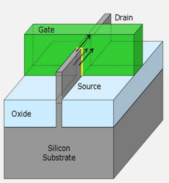
The basic FinFET layout in ideal form looks like this:

The active gate area is the intersection of the Green-color gate material and the arrows, showing direction of current flow. As a 3D structure the layout area of a FinFET is smaller than a planar device, and the source-drain region is fully-depleted for FinFET, making for:
- Reduced leakage transistor compared to planar CMOS
- Less variability
- Lower operating voltages
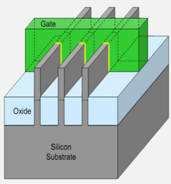
Multiple fins are required to get different effective widths for a FinFET transistor, so the device sizing is quantized instead of totally variable:

On the down-side with a FinFET technology you have some new circuit design trade-offs:
- Quantized widths
- No body biasing to control leakage or speed
- Higher parasitic values
- Aging and self-heating effects
Foundries offering FinFET technology today include:
- TSMC (16nm, 16nm+)
- Samsung + GLOBALFOUNDRIES will offer a common FinFET process at 14nm.
- Intel at 22nm and 14nm, FPGA vendor Altera is using an Intel 14nm FinFET process, while Xilinx is using the TSMC 20nm and 16nm FinFET processes.
- UMC 14nm
Technology reasons to choose FinFET include performance, where a 16nm FinFET is about 30% faster than a 28nm planar CMOS transistor. Leakage current in FinFET can be one half that of planar CMOS, which then allows for even smaller Vt values, which helps lower Vdd values, finally reducing overall power. It’s even possible to design FinFET-based SRAM circuits that operate at 500mV.Related: Intel 14nm is NOT in Production Yet!
Area reductions in SRAMs when going from 28nm planar to 16nm FinFET are up to 40%.
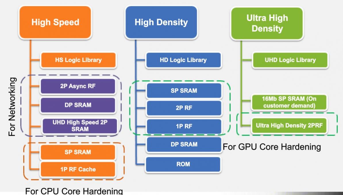
Synopsys EDA software and IP have been used to implement SoCs in all four FinFET processes (Intel, TSMC, UMC, Samsung). Here’s the list of FinFET-based IP from Synopsys where you can choose to tradeoff speed versus density to match your requirements:
 Related: USB 3.0 IP on FinFET may stop port pinching
For FinFET costs you have to deal directly with each foundry and make your own decision on the benefits and ROI.
Failure mechanisms in FinFET are different than with planar, so the memory redundancy approach and BIST changes. For example, you should be checking for resistive shorts and opens between fins. SER (Soft Error Rates) for FinFETs look better than with planar so far, so stay tuned for results from radiation labs.
Early adopters of FinFET technologies are those market segments with:
- Highest volumes and margins to justify increased costs.
- Power reduction requirements.
- Performance improvement needs.
My favorite phrase “techonomics” from Aart DeGeus wasn’t used in this webinar on moving to FinFET technology, although the concept was the same. Migrate to FinFET technology if it makes technical and economic sense for your market segment.
Q&A
Q: Does area reduction consider double patterning?
Yes, it does. DPT adds complexity to circuit designers and providers of IP.
Q: How many gates does it take for SMS Memory BIST to support FinFET-specific failures?
No extra gates are required for BIST, it’s all done in software.
Q: What speeds are you able to achieve on FinFET processes?
It’s design and foundry specific. Typically a 1.5GHz design at 28nm can now run at 3.0GHz in FinFET.
Q: Can I implement memory BIST from Synopsys with my own memory?
Yes, you can use Synopsys memory BIST on your custom memory, it’s been done before.
Q: Do you have any FinFET yield numbers?
You must contact your foundry directly, because that data is proprietary.
Q: How different are the FinFET SRAM defects?
FinFET defects are a superset of existing defects, so we’ve extended our algorithms to account for that. At ITC we have a paper this year on that topic.
Q: Which FinFET processes has Synopsys built IP on?
Our FinFET IP is ready today for all of the foundries talked about.
Q: How do FinFETs compare to FD-SOI?
That’s a long answer, so will be tabled for now.
Related: FD-SOI at 14nm
Q: What track heights will you support with logic libraries?
We offer high speed at 10.5 tracks, high density at 9 tracks, ultra-high density at 7.5 tracks.


Comments
0 Replies to “FinFETs for your Next SoC”
You must register or log in to view/post comments.