 Switching translates to power. Similar to the recent slow down experienced by Moore’s Law, the constant power density (power demand per unit chip area) prescribed by Dennard scaling was no longer affordable across the technological scaling. While the contribution of leakage power component in advanced process nodes was getting somewhat rectified recently, managing the dynamic power attributed to the increase device density is still a challenge as it is critically demanded by many mobile, IoT and data center applications.
Power, Clock and PowerPro
Dynamic power is defined to be proportional to frequency as given by the equation:  ; where k is switching activity, f is design frequency, c is capacitance and Vdd is operating voltage. Aside from memory, the clock network has been the major contributor to the overall power number as it is typically the largest net sprawling across the design and operates at the highest frequency of any signal within the entire synchronous system.
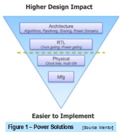 The traditional approach of power saving involves controlling switching of the clock network by inserting clock gating, which can be performed either at the RTL capture stage or during the synthesis stage through logic inferencing. On there other hand, there are many logic implementation styles such as in sharing common enable signals, applying derivative clock trees or free-running clocks, among others, hence, addressing a power optimal clock-tree implementation early is key in order to yield the greatest saving impact and to prevent unnecessary undoing of coded RTL as illustrated in Figure 1.
Since design-for-power methodology demands a rather holistic and converging solution, the availability of a solution that could identify a power optimal RTL code early, accurately assess and propagate the incurred power amount throughout the implementation stage is desirable. Mentor’s PowerPro has an integrated platform addressing such needs.
PowerPro has been the solution leader in RTL power optimization domain for the last few years. It provides a complete solution for measuring and optimizing power through an interactive exploration at the microarchitectural level. PowerPro is capable of spotting power leakage and applying opportunistic clock gating insertion during the RTL development cycle, while its physical-aware flow provides the necessary accuracy for estimating design power values. Its guided power reduction includes the recommended RTL codes that would satisfy the power saving and automatically validated by its built-in formal equivalency engine.
Alchip, CTS and Fishbone
Alchip® is a fabless ASIC provider serving various computing market segments and utilizes advanced process nodes to do IC design. In an attempt to further reduce power consumption on high performance designs, they have ventured into applying PowerPro solution on the clock tree implementation.
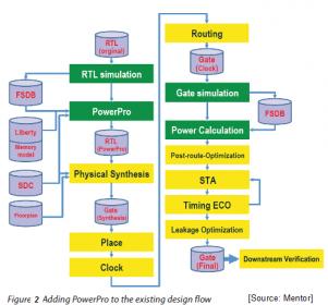 Clock network implementation can be categorized into two major types. as a tree structure or in gridded/mesh form, with some variations in between. The amount of shared network branches, connecting the a clock driver (root) to the sink points determines if the implementation is closely resembled to the conventional clock-tree network. As part of clock-tree implementation, CTS (Clock Tree Synthesis) is usually presented as an embedded P&R tool function as illustrated in the diagram Figure 2.
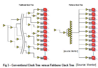
A 16nm, 600Mhz core processor design was used as a test vehicle using this flow. Two different clock topologies were applied: a conventional CTS and a fishbone clock tree as shown in Fig. 3. Only the total power numbers of two critical design entities: the flops and design clock network were compared as the power contribution from logic network or memories are effectively unchanged.
Sequential and Memory Clock Gating
Sequential clock gating requires the use of sequential analysis over multiple clock cycles to identify writes that are either unobservable down-stream or the same value is written in consecutive cycles. Deep sequential analysis has enabled PowerPro to take advantage of subtle RTL coding inefficiencies such as unused computations, data dependent function and don’t care cycles. It could disable previous cycle register data generation if data is not used in the current cycle.
Two prominent sequential clock gating techniques adopted by PowerPro: an Observability based Clock Gating in which scenario a change in a signal value does not propagate to a primary output/flop/latch/memory and does not affect the primary outputs (redundant writes that will not be used in subsequent clock cycles).
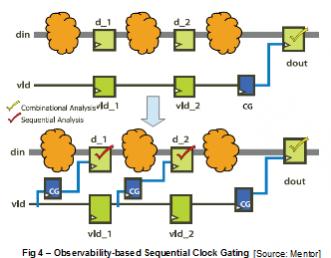
In the example on Fig.4, the circuit was a three staged pipeline data path containing 5 flip-flops. Under the combinational clock gating condition, only the last flip flop was gated and data flows through two computational stages before being latched into the output register dout. The output of doutis held based on the signal vld_2. Through combinational analysis, the clock gate on doutis added as a simple combinational substitution of the feedback loop. Sequential clock gating on both d_1and d_2requires a sequential analysis to propagate the data hold condition backwards, disabling the unused computations in previous cycles.
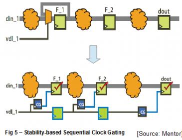
As illustrated in Figure 5, the second type is called Stability-based Clock Gating, which is when the same value as in the previous clock cycle is getting latched into a flop/latch such that it will not have any effect on the primary output. Although all of these analyses can be done vector-less, it can take user’s provided activity vectors through various formats (QWAVE, SAIF, FSDB) for further refined results.
Aside from flip-flops, memory components are prone to redundant toggles, as only a few memories are ON at any time. These can be reduced by means of similar coding techniques. The SRAM enable was intentionally left uncontrolled to represent the worst-case scenario for memories. PowerPro showed that it could automatically detect the enable signal and gated the SRAM properly by applying both the Observability-based and Stability-based clock gating –to resolve redundant read and write operation respectively– saving the memory’s dynamic power significantly.
Result Summary
There was an increased of 28% more clock gating covering over 68% of flip-flops compared with only 53% without PowerPro as captured Table 1. The additional clock gating cells did not adversely impact the design, instead it decreased the average toggling percentage on the output of integrated clock gatings (ICG) from 92.7% to 65.1%.

A significant reduction of power was reflected in total power for registers (26% less) and memories (80% less) as shown in the Table 2.

When PowerPro application was combined with the fishbone architecture, the overall impact is more pronounced of 59% total power reduction. Both the pre and post layout power numbers were also shown to correlate well: 31% post-layout vs 26% @ RTL for FF and 86% post-layout vs 80% @ RTL. PowerPro results were produced in the context of the RTL code, schematic display, design hierarchy representation and various sortable reports to enable efficient analysis and easy power tracking throughout the design cycle. It also accommodates the ECO flow by non-disruptive validation of post-ECO generated gate-level netlist to assess power.
Key takeaways from this case study: Mentor’s PowerPro allows power exploration and significant power optimization at micro-architectural level. Its pre-layout/RTL level power estimation shown with Alchip’s testcase to be within 6% compared with post-layout for both memories and sequential cells. The embedded equivalency checking facilitates an optimal RTL code that is correct-by-construction, thus helps ensuring convergence during design implementation. Such process agnostic power optimization should provide good starting point for power sensitive design as we head into 7nm process node and beyond.
For more details on PowerPro check HEREand Alchip case study and others please check HERE.
Share this post via:


Comments
There are no comments yet.
You must register or log in to view/post comments.