





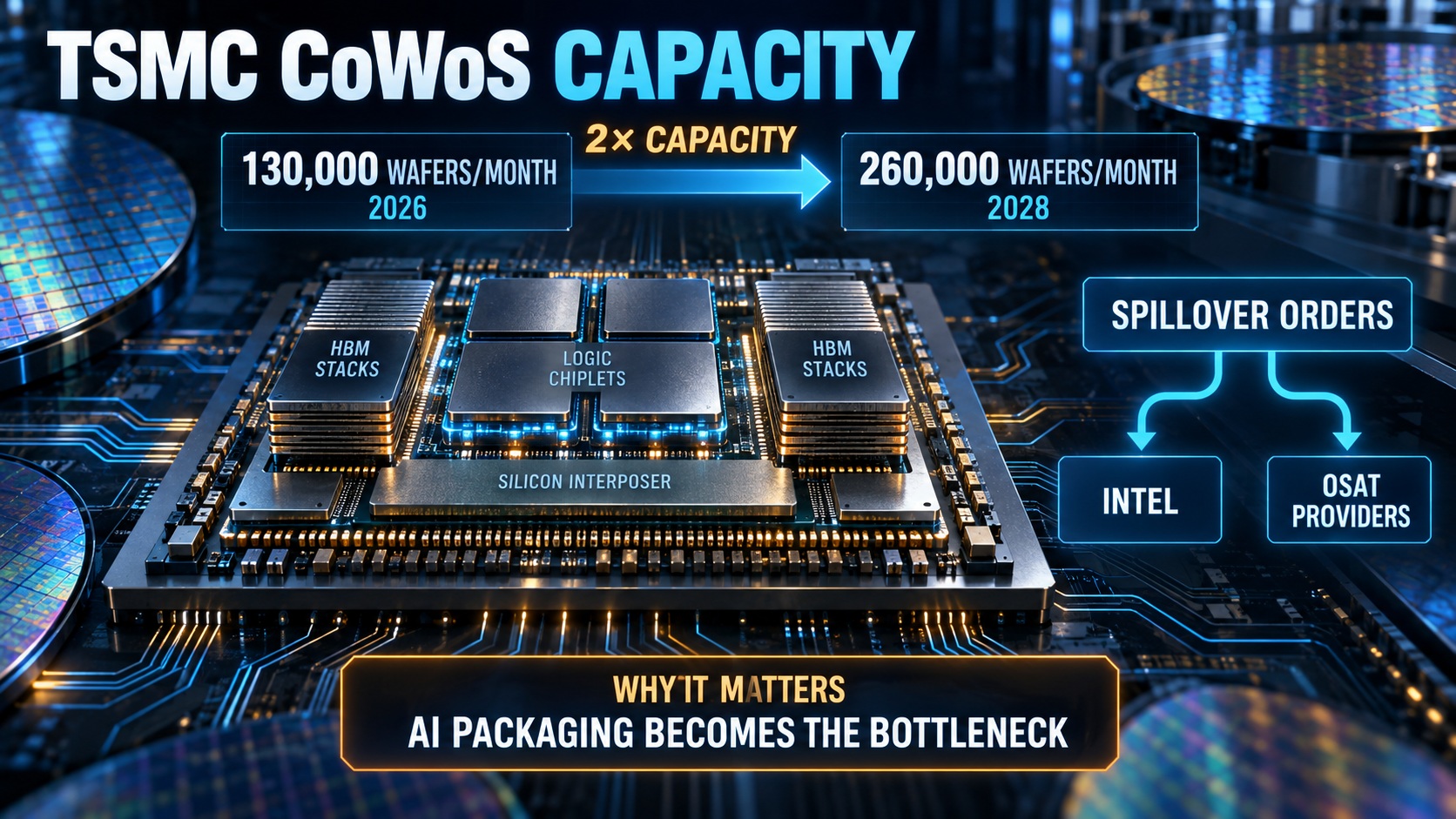
TSMC reportedly plans to double its Chip-on-Wafer-on-Substrate capacity from approximately 130,000 300mm-equivalent wafers per month at the end of 2026 to 260,000 by 2028. The estimate is not formal company guidance and should be treated as a supply-chain projection. Nevertheless, the direction is consistent with TSMC’s aggressive investment in advanced packaging and indicates that artificial-intelligence infrastructure demand is evolving from a temporary shortage into a multiyear capacity cycle.
CoWoS is a family of 2.5D packaging technologies that places logic dies—such as GPUs or custom accelerators—and high-bandwidth memory on a silicon interposer or redistribution-layer structure. The components communicate through dense, short interconnects before the assembly is mounted on an organic substrate. Compared with routing signals across a conventional circuit board, this architecture provides much higher bandwidth, lower latency and better energy efficiency.
That makes advanced packaging essential to AI performance. Leading accelerators require several HBM stacks to keep thousands of compute units supplied with data. A faster processor has limited value if memory bandwidth, interconnect density or power delivery cannot scale with it. CoWoS therefore is not simply the final step after wafer fabrication; it increasingly determines how much useful compute can be extracted from leading-edge silicon.
Package dimensions are also expanding. TSMC says it certified a CoWoS solution supporting interposers measuring 5.5 times the maximum mask or reticle area in 2025, with volume production planned for 2026. Larger packages can accommodate more compute chiplets, input/output dies and HBM stacks, but they consume more interposer area and packaging resources per device. Consequently, doubling wafer-equivalent capacity does not necessarily double the number of completed accelerators. TSMC’s 2025 annual report also identifies CoWoS, InFO and SoIC as central technologies for large-scale, power-efficient integration.
The expansion should help Nvidia, AMD and custom-ASIC developers raise shipments, yet it may not eliminate the shortage. AI clusters are moving toward larger multi-die packages, while hyperscalers are developing internal accelerators alongside purchases of merchant GPUs. Demand is therefore increasing in both volume and packaging intensity. Yield management, HBM availability, substrates, thermal solutions and testing capacity can remain bottlenecks even when nominal CoWoS output rises.
This imbalance creates an opening for Intel Foundry. Intel’s Embedded Multi-die Interconnect Bridge places small silicon bridges inside the package substrate instead of using a large interposer beneath every die. Foveros adds vertical die stacking, while EMIB-T combines bridge-based connections with through-silicon vias for improved signal and power delivery. These technologies are not drop-in replacements for every CoWoS design; customers must qualify physical interfaces, assembly processes, thermal behavior and reliability. But they offer an alternative route for new custom accelerators. Intel has confirmed that its advanced-packaging portfolio includes EMIB, EMIB-T and Foveros, while MediaTek has publicly said it supports both Intel and TSMC packaging platforms.
Outsourced semiconductor assembly and test providers should capture spillover as well. ASE, Amkor and other OSAT companies can perform portions of package assembly, bumping, substrate integration and final testing, either through cooperation with foundries or through competing 2.5D platforms. Amkor’s Arizona advanced-packaging campus, scheduled to begin production in 2028, illustrates how packaging demand is also encouraging geographic diversification.
Bottom line: Semiconductor leadership is no longer defined solely by transistor density. The ability to combine heterogeneous dies, HBM and high-speed interfaces at acceptable yield and cost now determines accelerator supply. TSMC’s expansion reinforces its leadership, but persistent demand gives Intel and OSAT providers something equally valuable—production orders, customer qualifications and the opportunity to become permanent second sources rather than temporary overflow suppliers.
We will get an update next week at the TSMC OIP Forum but this is where we are at today. Simply incredible, absolutely.
Also Read:
TSMC’s 2026 OIP Forum to Spotlight the Technologies Shaping the Next Era of Chips
Comparing Advanced Packaging from TSMC, Intel Foundry, and Samsung Foundry
Comparing Intel EMIB and Intel Foveros
Share this post via:



Comments
There are no comments yet.
You must register or log in to view/post comments.