"Managing increasing complexity through higher-level of abstraction: What the past has taught us about the future" Dr. Ajoy Bose, Atrenta CEO
Here is the abstract:
Time to market and design complexity challenges are well-known; we have all seen the statistics and predictions. A well-defined strategy to address these challenges seems less clear. Strategies to optimize the chip implementation flow, including approaches such as transistor-level optimization abound. While these techniques contribute to the solution, they all miss the primary force of design evolution. Over the past 30 years or so, it has been proven time and again that moving design abstraction to the next higher level is required if design technology is to advance. In this keynote presentation, a new EDA model will be presented, examples of past trends will be identified, and an assessment will be made on what these trends mean in the context of the current challenges before us. A snapshot of the future will be presented which will contain some non-intuitive predictions.
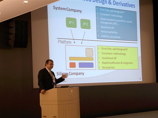
The talk basically looks at semiconductor design and EDA from a historical perspective and highlights that things always move to a higher level of abstraction to address complexity. IP was the most relevant example used as it continues to have a profound impact on the semiconductor design manufacturing ecosystem. You will be hard pressed to find a modern semiconductor design, in production today, without a reusable block, whether commercial or proprietary.
In fact, commercial semiconductor IP revenue jumped 30%+ in 2010, according to EDAC, and soft (abstracted) IP is a significant part of that number. Interestingly, semiconductor IP growth tracks nicely with semiconductor industry growth (30%+) and not EDA revenue growth (0%). Take a look at the SIP and EDA business models and you will see why (semiconductor IP is success based and EDA is not).
The talk also focused on platform based design and IP reuse as critical items to tame complexity and spiraling design cost. Ajoy then talked about a "new breed" of EDA company – called "5th generation EDA" to address these requirements. Check out the Atrenta newsletter HERE, it is a company you definitely want to watch!


Intel High NA Adoption