The semiconductor industry is experiencing a significant transformation with the advent of chiplet design, a modular approach that breaks down complex chips into smaller, functional blocks called chiplets. A chiplet-based design approach offers numerous advantages, such as improved performance, reduced development costs, and faster time-to-market. This approach improves yield by isolating defects to individual modules, optimizes transistor costs by allowing different manufacturing nodes for different components, and leverages advanced packaging technologies for enhanced performance. The modularity of chiplets supports scalable, customizable designs that accelerate time-to-market and enable targeted optimization for performance, power, and cost.
However, one of the most substantial barriers to widespread adoption has been the lack of standardization in how these chiplets communicate with each other. The Universal Chiplet Interconnect Express (UCIe) standard is poised to change that, making chiplet design more accessible and opening up new opportunities for innovation across the industry. Mayank Bhatnagar, a Product Marketing Director at Cadence gave a talk on this subject at the FMS 2024 Conference in early August.
Standardization and Interoperability
Before standardized chiplet interfaces, custom designs for each chiplet were needed, leading to higher costs, longer development times, and limited interoperability. Companies had to develop proprietary interfaces for their chiplets, making it difficult to integrate components from different suppliers. This lack of interoperability increased development costs and limited the pool of available chiplets.
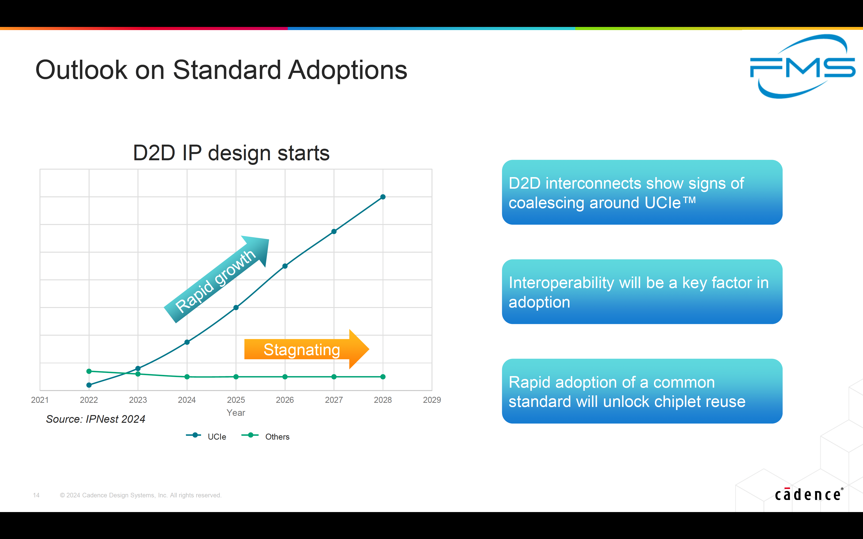
The adoption of standards simplifies this process, allowing designers to focus on core innovations while using pre-validated interfaces for communication. This reduces custom design efforts, accelerates development, and ensures seamless integration. Companies can now leverage proven chiplets, cutting costs and improving quality. Overall, standardization streamlines design, reduces resource use, and speeds up time-to-market. Over the recent past, a number of chiplet-to-chiplet interface standards have been developed.
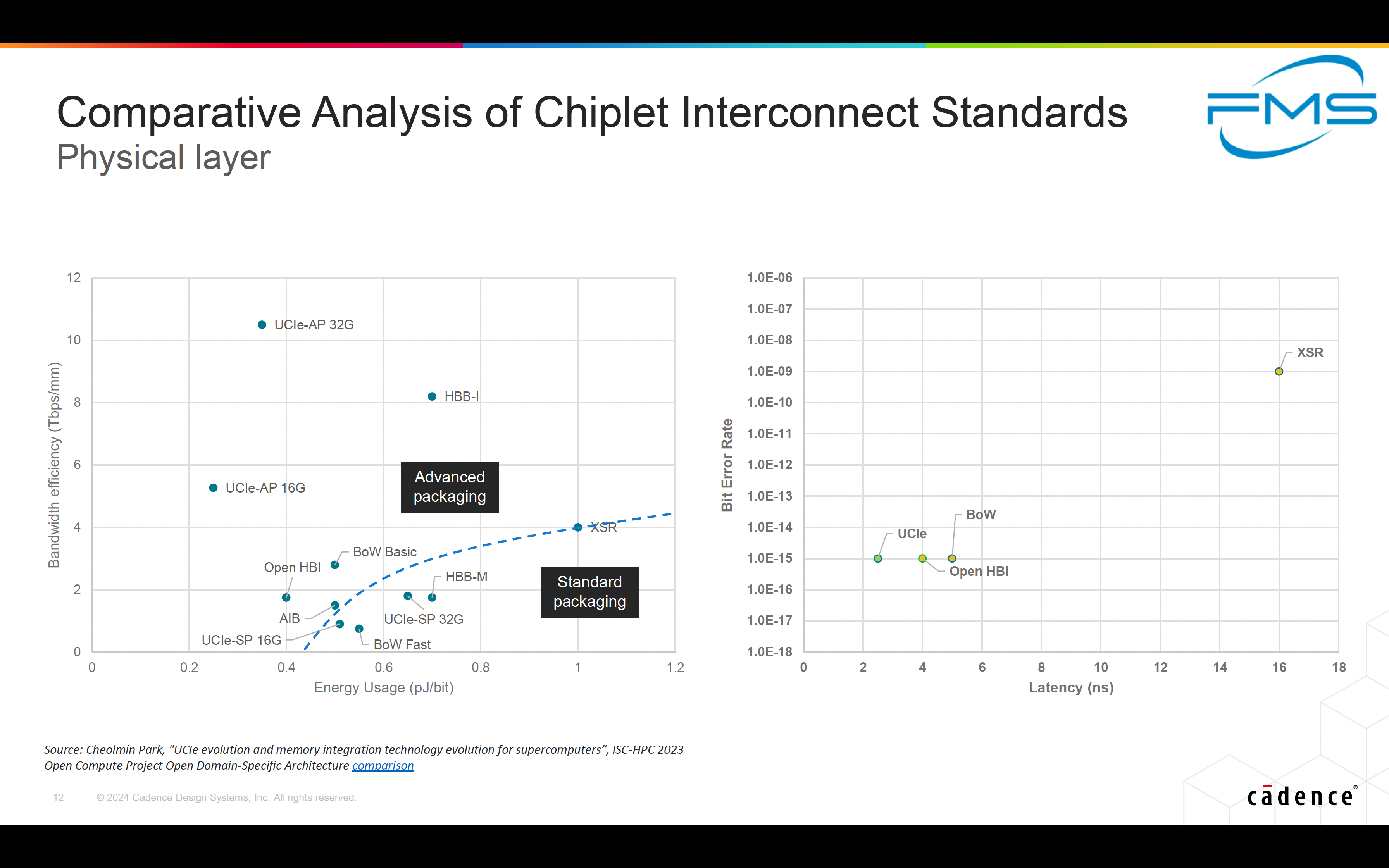
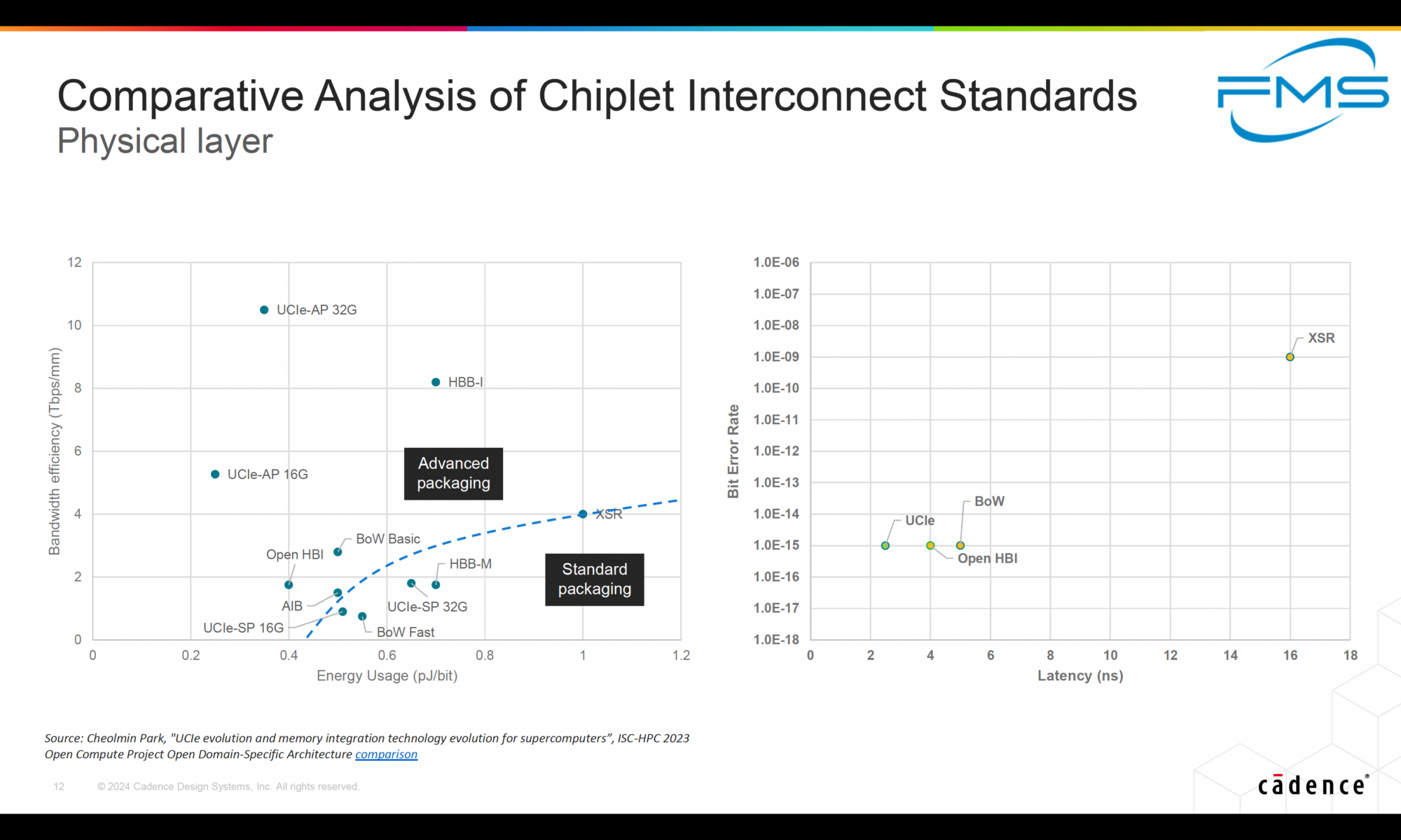
A comparative analysis of these various standards indicates that, in terms of bandwidth efficiency, energy usage efficiency and latency, UCIe excels.

The Role of UCIe in Chiplet Design
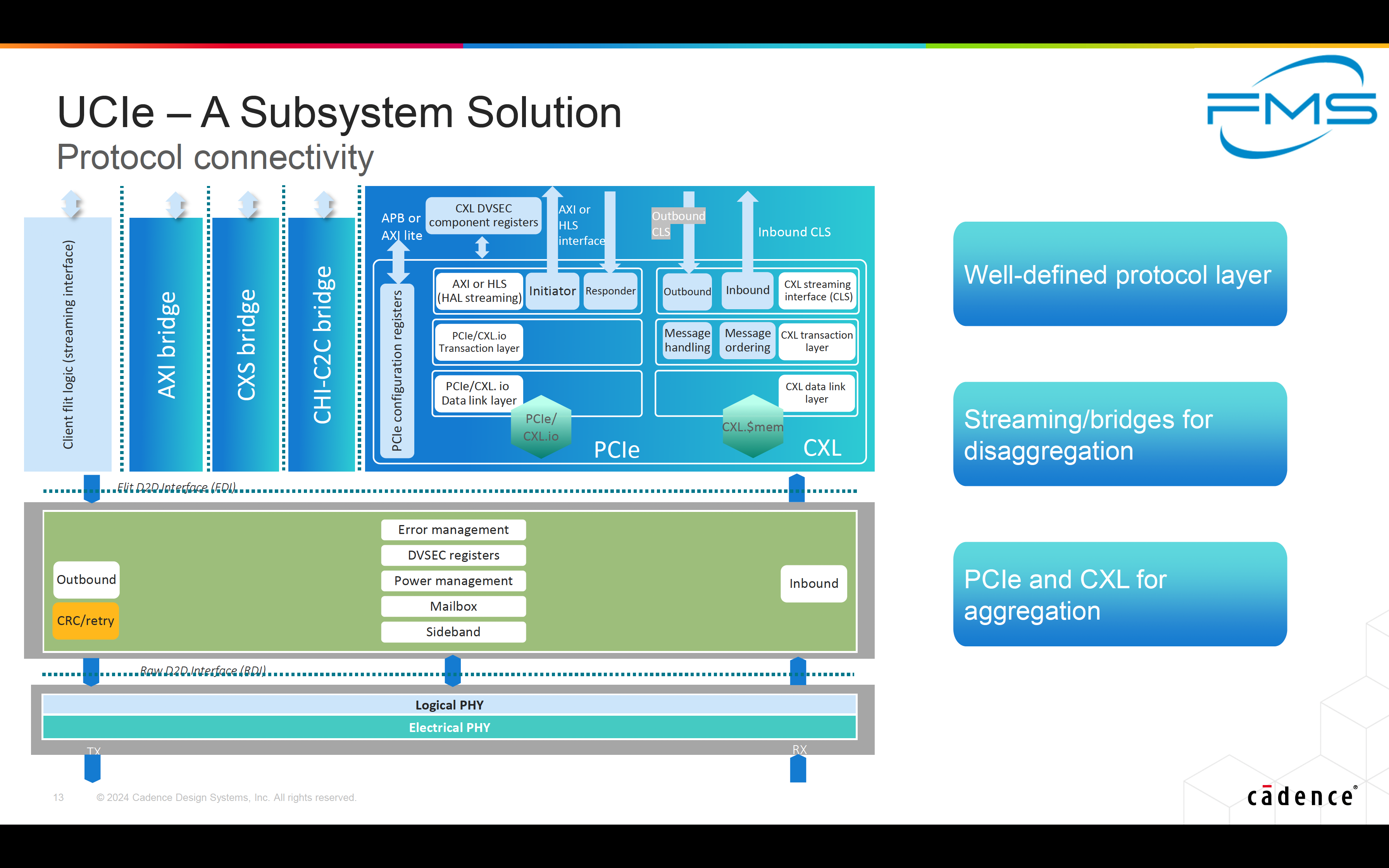
UCIe, or Universal Chiplet Interconnect Express, is an open industry standard that defines a high-bandwidth, low-latency interconnect protocol for connecting chiplets. UCIe provides a common interface for chiplets to communicate, much like how USB standardized peripheral connections in the PC industry.

With UCIe, companies can mix and match chiplets from various vendors, fostering a more competitive market and driving innovation. It lets designers focus on core innovations and highly customized cores and leverage standardized interfaces for the periphery. By surrounding highly customized cores with standard periphery, designers can maximize their market reach and efficiency.
Enabling Specialized and Customized Solutions
One of the most exciting possibilities enabled by UCIe is the potential for highly specialized and customized solutions. In the past, companies had to rely on expensive monolithic SoCs or resort to general-purpose SoCs that might not be perfectly suited for their specific application. With chiplets and UCIe, companies can build custom systems tailored to their exact needs, selecting the best components from a variety of suppliers. For example, a company developing an AI accelerator could choose a high-performance CPU chiplet from one vendor, a specialized neural processing unit (NPU) from another, and memory from a third. UCIe ensures that these components can communicate effectively, allowing the company to create a highly optimized solution without the need for an expensive monolithic custom SoC.
Custom Silicon for AI Applications
The demand for custom silicon is rapidly increasing, driven by the need to optimize hardware for specific AI applications such as training, inferencing, data mining, and graph analytics. AI training requires high-performance, parallel processing capabilities to manage large datasets and complex models, while AI inferencing demands low-latency, high-throughput processing for real-time predictions and decisions. Data mining benefits from custom silicon tailored for specific data processing and extraction tasks, and graph analytics requires chips designed to handle the complexity of graph processing and large-scale parallelism. A chiplet-based approach leveraging UCIe offers significant advantages for these applications in terms of performance, power efficiency, and scalability.
Fostering Innovation and Collaboration
As an open industry-standard, UCIe not only reduces barriers to entry but also encourages collaboration and innovation within the semiconductor industry. By establishing a common platform for chiplet communication, UCIe enables companies to focus on their core competencies, whether that’s developing cutting-edge processors, advanced memory technologies, or specialized accelerators. This collaborative environment can lead to the development of new, innovative products that might not have been possible within the constraints of traditional SoC design. As more companies adopt UCIe and contribute to the ecosystem, the variety and quality of available chiplets will continue to grow, further driving innovation.
Summary

UCIe represents a significant step forward in the evolution of chiplet design, lowering the barriers to entry for companies of all sizes. By standardizing the communication between chiplets, UCIe makes it easier for companies to develop custom, high-performance systems without the need for costly and complex SoC designs. As a result, UCIe is expected to democratize the semiconductor industry, fostering greater innovation and competition while enabling a new wave of specialized and customized solutions. The future of chip design is modular, and with UCIe, that future is more accessible than ever. The growing demand for custom silicon for AI applications will drive further advancements and opportunities around UCIe technology.
For more details, visit Cadence’s UCIe product page.
Also Read:
The Future of Logic Equivalence Checking
Theorem Proving for Multipliers. Innovation in Verification
Empowering AI, Hyperscale and Data Center Connectivity with PAM4 SerDes Technology
Share this post via:


Comments
There are no comments yet.
You must register or log in to view/post comments.