The concept of shift left is getting to be quite well-known. The strategy involves integrating various checks typically performed later in the design process into earlier stages. The main benefit is to catch and correct defects or errors at an earlier stage when it’s easier and faster to address. For complex SoC design, using this strategy can be the margin of victory. Siemens Digital Industries Software recently published a Technical Paper on deploying a shift left strategy for IP design. Called design stage verification, the paper provides an in-depth discussion on strategies and benefits for various IP design flows. The results can be dramatic. It’s a valuable document for anyone dependent on IP, which is just about everyone in chip design. A link is coming, but first let’s examine how design stage verification gives a boost for IP designers.
The Various IP Design Flows in Use Today
From a design perspective, there are basically three IP categories – hard, soft, and custom. Hard IP, such as cores and standard cells, are typically custom designs certified by a foundry at the time a process technology is defined. Soft IP typically consists of SRAM compiled from a library of pre-defined cells (bit cells, IO cells, etc.) to create the hard IP. And custom IP is typically created for a specific design, or to implement functionality that is patented or provides a competitive advantage. Traditional custom IP cell design requires manually creating a layout in a custom editor.
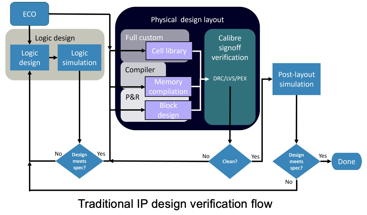
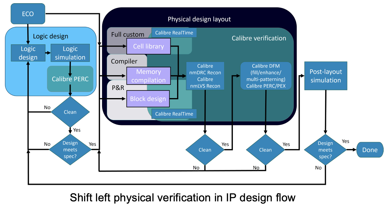
All of these methods require several forms of validation such as DRC and LVS to ensure the design is correct and compatible with the target foundry process. The Calibre family of products from Siemens is the industry leader in this area, so the technical paper naturally covers the most popular and trusted strategies for verification. The figures below summarize the traditional IP design verification flow and which Siemens tools are added to implement a shift left version.


Let’s examine some details about these flows and the benefits of shift left.
How Design Stage Verification Boosts the Process
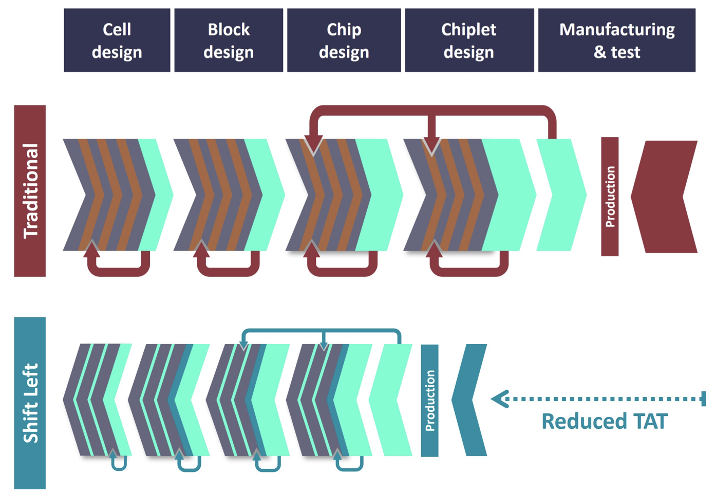
A shift left methodology will enable design teams to enhance productivity and design quality while reducing time to market, as shown in the figure below. Note achieving these improvements requires coordination between design of low-level IP, macro blocks and the top-level SoC. A lot of moving parts and a lot of complexity to manage.

The Technical Paper does a great job explaining how to implement a shift-left methodology for the various IP design flows. I highly recommend you download it and get a first-hand look. To give you a sense of the scope of the document, here is a list of activities that are discussed in detail:
Targeted verification: The Calibre nmDRC Recon and nmLVS Recon tools provide automated ruleset selection that focuses on running rule checks for rules with local scope that target critical and systemic errors. By running these targeted checks during early design stages, designers can not only significantly reduce runtimes, but also generate results that are geometrically close to the source of the issue, reducing debug time as well.
On-demand DRC verification: The Calibre RealTime Digital and RealTime Custom tools are integrated with all major design and P&R tools. The Calibre RealTime tools provide immediate feedback for DRC violations in the design or implementation tool. This feedback enables designers to quickly analyze and correct DRC errors using Calibre signoff engines and rule decks, ensuring any fixes remain DRC-compliant.
Integration and runtime invocation: The Calibre Interactive interface supports the integration of Calibre tools into design and implementation environments and enables automated PV flows by providing user-friendly configurable interfaces for run set invocation, as well as automated pre- and post-run operations.
Debug integration and guidance: The Calibre RVE results viewer provides error debugging within all major design and implementation environments, enabling design engineers to work in a familiar design cockpit to debug and correct errors. Automated error categorization and filtering capabilities help designers perform targeted debugging in a systematic way by organizing results based on most likely root cause.
Automated waiver management: The Calibre Auto-Waivers® tool can be used in conjunction with the Calibre nmDRC Recon tool to define and maintain design rule waivers in collaboration with IP library providers and the foundries, all within a familiar PV environment.
Pattern matching: Symmetry in IP design is a core component of IP quality. The Calibre Pattern Matching tool simplifies complex design requirements through interactive pattern-enabled checking. Verifying transistor or even complex multi-layer device symmetry is a point- and-click check accessible directly in the layout design environment.
Reliability verification: The Calibre PERCTM reliability platform provides a powerful suite of electrical checks combined with the ability to apply context-aware checking that enable IP designers to find and eliminate reliability impacts such as electrostatic discharge (ESD) and latch-up during early design stages, reducing the time and resources needed to capture these issues in simulation.
Automated design layout optimization: Design for manufacturing (DFM) optimization consists of design adjustments that are not required, but that can improve a design’s manufacturability and/or performance and reliability. While DFM optimization traditionally occurs during signoff verification, the Calibre DesignEnhancer® tool offers three use models that enable designers to apply selected automated DFM optimizations during early design stages.
Advanced fill functionality: Calibre YieldEnhancer SmartFill and engineering change order (ECO) fill capabilities allow designers to maintain most of their timing analysis when an ECO occurs. Calibre YieldEnhancer programmable edge modification (PEM) uses layout analysis to move edges or polygons to optimize manufacturability.
Multi-patterning color assignment: Coloring assignment for multi-patterning is an important aspect in IP design because block/full chip designers must be able to color IP cells correctly in many various orientations and configurations.
To Learn More
This is just a summary of a lot of detail that is well-covered in this new Technical Paper from Siemens. You can download your copy of the complete document here and learn why design stage verification gives a boost for IP designers.
Share this post via:


Comments
There are no comments yet.
You must register or log in to view/post comments.