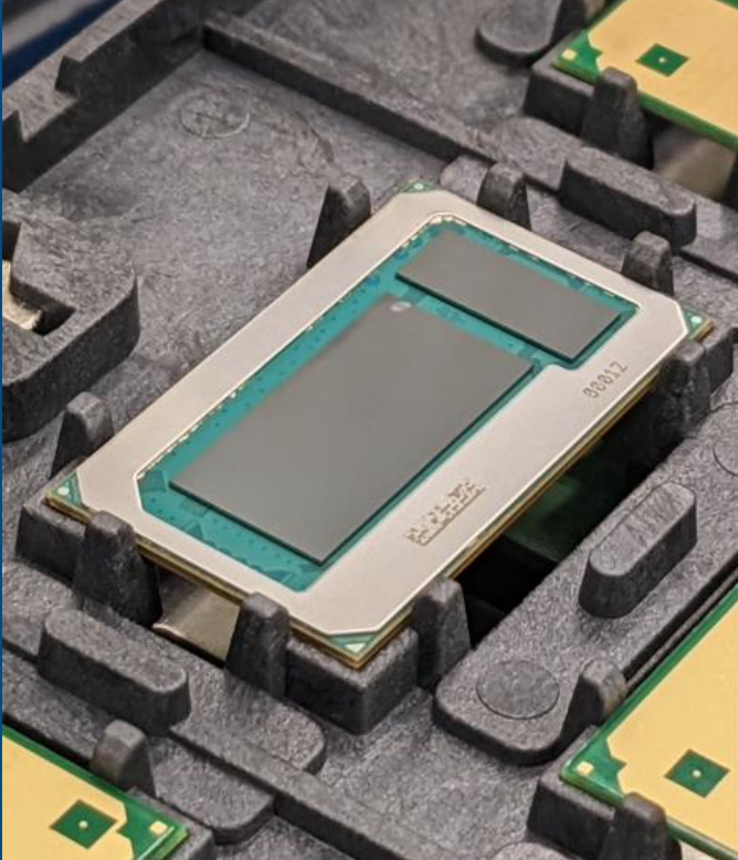
Intel recently issued a press announcement that has significant implications for the future of semiconductors. The release announces Intel’s new glass substrate technology. The headline states: Glass substrates help overcome limitations of organic materials by enabling an order of magnitude improvement in design rules needed for future data centers and AI products. This should definitely get your attention. I had the opportunity to get a pre-briefing that went into a bit of the backstory on this new development. Read on to understand how Intel ushers a new era of advanced packaging with glass substrates and why it matters.
The Briefing

Details say a lot. As I logged into the pre-briefing presentation on Intel’s glass substrate technology, I looked at the attendee list. It was a virtual Who’s Who for just about every high-power market analyst and researcher. When Intel talks, the world listens. The briefing was presented by Rahul Manepalli, Intel Fellow & Senior Director of Substrate TD Module Engineering. Rahul has almost 24 years of tenure at Intel. During his introduction, it was explained that Rahul and his team are responsible for the development of the next generation of materials, processes and equipment for Intel’s package substrate pathfinding and development efforts. Quite a lot of responsibility. Rahul has a Ph.D. in Chemical Engineering from the Georgia Institute of Technology. He has a substantial command of what’s happening at Intel, and his presentation was simultaneously easy to understand and very rich in technical details. This is a rare set of skills.
The highlights of Rahul’s presentation were:
- Intel’s breakthrough achievement enables continued scaling and advances Moore’s Law
- Glass substrates enable an order of magnitude improvement in design rules needed for future data center and AI products
- Chip architects can pack more “chiplets” in a smaller footprint on one package
- Improved density and performance properties will lead to lower overall cost and power usage
Glass substrates took center stage for the discussion. The resulting packaging technology will enter the mainstream later this decade. Given the long lead time. don’t underestimate the impact this technology will have. There is currently an electrically functional, assembled MCP test vehicle with three layers of RDL and TGV of 75um. The photo at the top of this post is the test vehicle.
Some Details
It turns out Intel has been leading the way in advanced package design for quite a while. In 1995, the company led the transition to organic substrates. That was followed by Intel’s invention of embedded multi-die interconnect bridge, or EMIB. Intel leads the way again with the introduction of glass core substrates.
Glass core substrates offer substantial improvements in packaging technology when compared with organic substrates. Like organic materials, glass can be fabricated in a variety of sizes. Rahul explained that organic substrates are a composite material. Glass, on the other hand, is a homogenous amorphous material. This allows Intel to tune the properties of the glass substrate to bring it closer to the properties of silicon. This opens up the opportunity for many performance and density enhancements – the order of magnitude improvement in design rules mentioned earlier.
Benefits exist along both electrical and mechanical axes. Rahul provided the following summary:
- Tunable modulus and CTE closer to silicon → large form factor enabling:
- Dimensional stability → Improved feature scaling
- High (~10x) through-hole density → improved routing and signaling
- Low loss → high speed signaling
- Higher temperature capability → advanced integrated power delivery
Rahul also shared some more details about the improvements glass substrates deliver over organic:
- Tolerance for higher temperatures offers 50% less pattern distortion
- Glass substrates have ultra-low flatness for improved depth of focus for lithography
- Dimensional stability needed for extremely tight layer to layer interconnect overlay
- Up to 10x increase in interconnect density possible with glass
- Improved mechanical properties of glass enable ultra-large form-factor packages with very high assembly yields
- Glass provides improved flexibility in setting design rules for power delivery and signal routing
- Ability to seamlessly integrate optical interconnects, as well as embed inductors and capacitors into the glass at higher temperature processing
- Better power delivery solutions while achieving high-speed signaling that is needed at much lower power
Glass clearly opens the door to a new level of integration and performance. Rahul shared some information about how this is all done at Intel. The company’s work on glass goes back a decade. There is a fully integrated glass R&D line with over $1B investment in Chandler, AZ. Intel is working closely with equipment and materials partners to enable the ecosystem. To support demanding AI and data center applications, filled through glass vias with a ~20:1 aspect ratio for 1mm core thickness have been fabricated. As mentioned, there is an electrically functional, assembled MCP test vehicle. And Intel has over 600 inventions related to architecture, process, equipment, and materials. This is an impressive summary.
To Learn More
The press release has a lot of good information. In addition, there is a 3.5-minute video on Intel’s packing pedigree that is definitely worth a look here. And that’s how Intel ushers a new era of advanced packaging with glass substrates.
Also Read:
How Intel, Samsung and TSMC are Changing the World
Intel Enables the Multi-Die Revolution with Packaging Innovation
Intel Internal Foundry Model Webinar
Share this post via:


Comments
7 Replies to “Intel Ushers a New Era of Advanced Packaging with Glass Substrates”
You must register or log in to view/post comments.