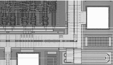
My wife and I have traveled to Switzerland on vacation and marveled at the natural beauty of the mountains, efficient train system, tasty chocolate, and wonderful foods. I only wished that our American dollar bought more in Swiss currency than it did. Recently I discovered a high-tech IC design company called Microdul that designs mixed-signal chips with ultra low-power specs in product areas like:
- Quartz clock circuits
- RTCs
- Medical implants
- Temperature sensors
- Humidity sensors
- Pressure sensors
- Capacitive, inductive and optical sensors
- Light barriers
- Locks and security systems
- Keyboards

I was able to have a phone discussion with three people at Microdul this week to learn more about their EDA tool flow as applied to a mixed-signal design and product business:

Dr. Phil Poole, Director of Semiconductors
Dan Liu, Mixed-Signal IC Designer
Wilfried Hasselberg, CAD Tool Flow and IC Designer
Questions
Q: How did Microdul get started?
Q:Microdul – 1991 we started in Zurich, Switzerland as a management buyout of a department of Philips Semiconductors AG Zurich. Phil joined in 2002 and started to create more ASIC products and mixed-signal. Medically certified with ISO13485 where devices are implanted into humans (both semi and module). Total number of people is 70 with multiple product lines. We are a privately held company, with no debt, and Microdul Holding AG includes: Microdul AG, Innodul AG and Aptifab AG as subsidiaries.
Q: How many chips does your team design per year?
A: Microdul is a management buyout from Philips Semi in the 90’s. We initially started off designing ASICS, now our IC design team is up to 10 people (3 on test), and we work on about 2-3 chips per year.
Q: What is the complexity of each design in terms of engineers, transistors, frequency and length of project?
A: Our IC design projects have a variable complexity, we are now doing some standard products in addition to ASICs. We have used a semi-custom approach in the past with the design of our own pre-fabricated analog arrays that worked OK but now we are starting to use a full-custom approach. We can design mixed-signal ICs using our arrays of 5K to 20K devices. Smaller designs may have 1K digital gates and hundreds of analog devices. Larger designs have 2.5K analog devices. Working with analog arrays is quicker time to market, while full-custom gives more flexibility.
Q: Do you re-use IP, and if so where does the IP come from?
A. There is some semi IP re-use when we can, like an oscillator for example. Our customers typically need something very specific so we have to start from scratch or re-size transistors for each process node selected. We are not using any automated transistor sizing approaches yet.
Q: What other simulation approaches have you used before?
A: We’ve used a simulator that allowed Digital Gates plus SPICE level before however as mixed-signal design sizes grew we needed a bigger simulator.
Q: Why did you want a change in simulation methodology?
A. We started using the SMASH simulator from Dolphin Integration for mixed top-level simulation because it was the only affordable alternative we found that could do this. We have only just started to use it for top-down simulation.
Q: What other simulators did you consider?
A: I looked at Mentor, Cadence and Tanner tools.
Q: Would you say that your simulation approach is a top-down, bottom-up or both?
A: We do both approaches. SMASH simulates both Digital Logic and Verilog AMS together. Tanner SPICE simulates our transistor-level blocks. A project manager for each chip design keeps us organized, and one engineer does both the top-level and verification of the design. Multiple engineers could be designing on a single chip and then they each do their own blocks. Example analog blocks include: oscillators, PLL, sensor interfaces, amplifiers, comparators, (low-frequency mixed-signal, ultra low power). Our foundry choices are: NXP and TSMC (for arrays), X-FAB (full-custom).
Q: Where are the Tanner tools used?
A: S-Edit for schematic capture, L-Edit for layout, T-Spice for block-level simulation, and HiPer Silicon for DRC/LVS of blocks and full chip.
Q: What about other EDA tools in your design flow?
A: For logic synthesis it’s Incentia, on the DFT side we use Syntest.
Q: What OS do you use?
A: For the Tanner tools it’s Windows 7 while everything else runs on Linux with Red Hat 6.
Q: Just how low power are your designs?
A: One of our Oscillator designs uses only 60nA, which is a very low power spec.
Q: What is an analog design challenge that you have solved?
A: One challenge would be in designing a low jitter number for our PLLs.
Q: When silicon comes back from the fab does it always work to spec the first time, if not why not?
A: We do both a wafer-level or final test of packaged parts. Some parts are sold as die, others as packaged parts. Our digital testing flow is well developed. The analog part of test is design-specific and there the challenge is to make analog controllable and observable. We have our own test engineers and test equipment, however for larger quantities the parts can be tested in the Far East. First silicon we mostly get functional samples, about a 90% success rate and then some tweaking for the 2[SUP]nd[/SUP] silicon. About two spins for perfection. With the analog arrays a spin can be complete in 6 weeks using only metal customization. Our full-custom IC design has yet to tape out.
Q: Where do your chip designers come from?
A: Wilfried is German, Dan is Chinese, then we have engineers that are American, French, Spanish, Portuguese, and Swiss.
Q: Can you quantify the benefits of using Tanner and SMASH tools together versus what you have tried before? Are you finding more bugs sooner? Less silicon spins, etc?
A. Our newest project is full-custom and it is a non-trivial design in progress. The chip has low power oscillators, digital logic, new functions, battery life detectors, power management, and 10K gates of FSM (Finite State Machine). Our technology choice is CMOS. The watch industry is the use for this new chip. The mixed-signal nature and complexity of the design required us to use the SMASH simulator and Tanner schematic and customer layout tools.
Q: How do you calculate power consumption?
A: For power calculations we simulate with SPICE. The leakage currents reported by SPICE are more pessimistic than actual silicon but it gives us a good idea that we met our spec.
Q: Are the foundry PDKs specific to Tanner or iPDK? Why?
A: For now the PDKS are specific to Tanner tools. In the future we will start to use the iPDK as Tanner works with popular foundries.
Q: What would success look like in 2012 for Microdul?
A. Success this year will be to get 1[SUP]st[/SUP] silicon back in December that works to spec the first time.
Summary
Microdul is a successful and growing mixed-signal IC design company with both products and services serving a variety of low-power end markets. They mix tools from multiple EDA vendors including: Tanner EDA, Dolpin Integration, Syntest, and Incentia.


Comments
There are no comments yet.
You must register or log in to view/post comments.