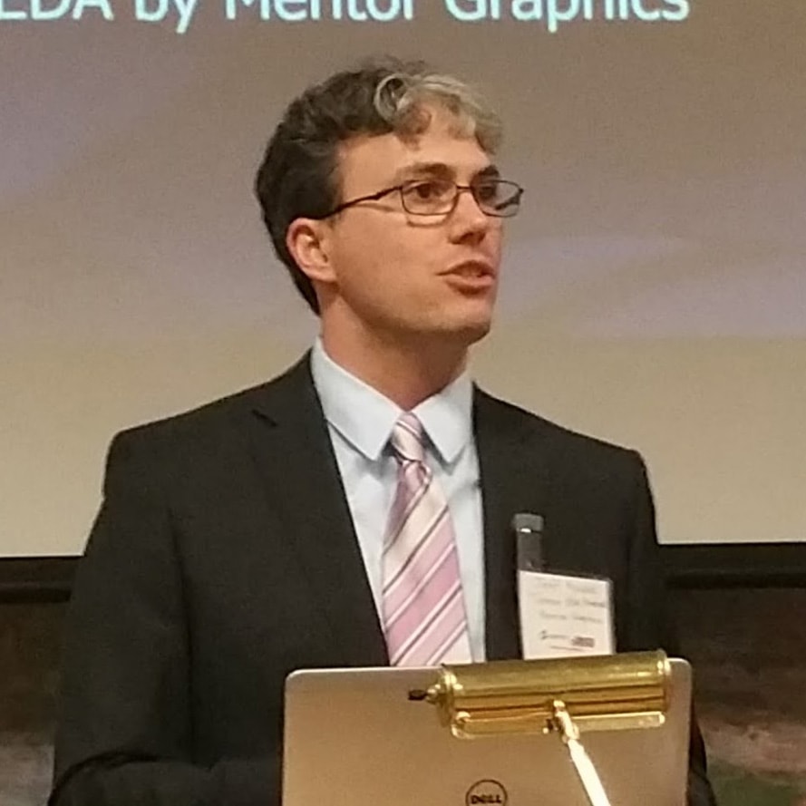

Last Friday I learned something new about IoT by attending a SEMI event in Wilsonville, OR just a few short miles away from where I live in Tualatin. SEMI puts on two events here in Oregon each year, and their latest event on IoT Sensors was quite timely and popular judging by how many attendees showed up. First up was Jeff Miller from Tanner EDA, now owned by Mentor Graphics.

Jeff tried to quantify the market size for IoT by citing sources like Infosys that predict a $300B market, while Cisco Systems sees a much larger $14.4T market size. Big number forecasts attract a lot of vendors, but where do they all play? There are several segments that make up IoT:
- Server Network Center
- Gateways
- Sensors/Actuators
Related blog – Why did Mentor Acquire Tanner EDA?
The edge of the IoT is mostly analog and it’s a multi-physics world, so us traditional EE majors need to learn how to speak with ME majors too. MEMS is a technology much used in IoT for sensing, uses multi-physics, has unique packaging, however there are few process standards especially when compared to the silicon foundry business model.
One of the most popular product example is the MEMS microphone sensor, used in most smart phones today with some 8 billion unites shipped to date. The microphone packaging is exposed to the elements and the mechanical portion is a membrane design. You must run simulations for air damping and acoustic signal propagation, then integrate some audio signal processing.
Another MEMS example would be with integrated photonics to monitor strain on a building or bridge. Image sensors are also heavily used in IoT devices ranging from the Mars Rover to automobile imaging systems. When we start using analog features in silicon for IoT devices then there can be higher voltages involved than with typical logic processes.
In general the IoT Edge requirements are: high volume, low cost, small size, and low power. Many IoT devices are using sensors which then require analog signal processing, A/D converters, D/A converters, actuators, controllers and even radios so that a gateway can be used to send data into the Cloud. An IoT design can be built with at least three styles:
- Components on boards
- Using advanced packaging
- On-die integration
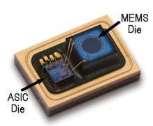
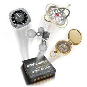
An example of advanced packaging is where multiple die are assembled into a single package using an MCM approach like when InvenSense created a 3-axis gyro, altimeter, magnetometer where 3 dies are placed together in a single package.
MEMSIC has an example where and accelerometer is combined with a logic IC into a single chip. Our modern autos use a tire pressure monitoring system from Sensata Technologies that has a MEMS pressure sensor and RF logic to communicate with the auto information system, having shipped some 325 million units so far.
Who is actually building out IoT today? Well, many players really: systems companies, cloud players. start-ups, even semiconductor vendors.
Tanner EDA has been offering EDA tools for analog and MEMS designers for some 28 years now, and now that they’re integrated into Mentor Graphics they can even offer of what an IoT engineer team needs in terms of a RTOS like Nucleus or PCB software like PADS.
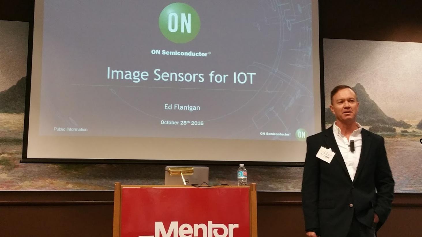
ON Semiconductor
Ed Flanigan spoke to us about image sensors and the role that they play in IoT. In humans we use up some 80% of our brain power on vision alone, so it’s a tough problem for both humans and silicon. ON Semi predicts that sensors will grow to 1 trillion units by 2025 where Imaging is #1, inertial sensors are #2, magnetic is #3 and pressure is #4 in importance.
The human eye is quite complex with about 1 million neural fiber connections to the brain, where an inverted image is flipped right-side up by the brain and focused. We have blue/green and blue/yellow receptors, no red sensors, however the brain creates the red color.
Image sensors used in wearables have performed tasks like heart rate monitoring in a product like the Apple Watch. Google presented a paper on their work to create a glucose sensor inside of a contact lens device for diabetics that need daily measurements. There’s even a swallow pill cam that can take 30 fps videos inside your body.
Automotive is a huge growth area for image sensors fueled by the demand to assist human drivers all the way up to self-driving cars. ON Semi has products that help out in the ADAS and auto image sensing markets.
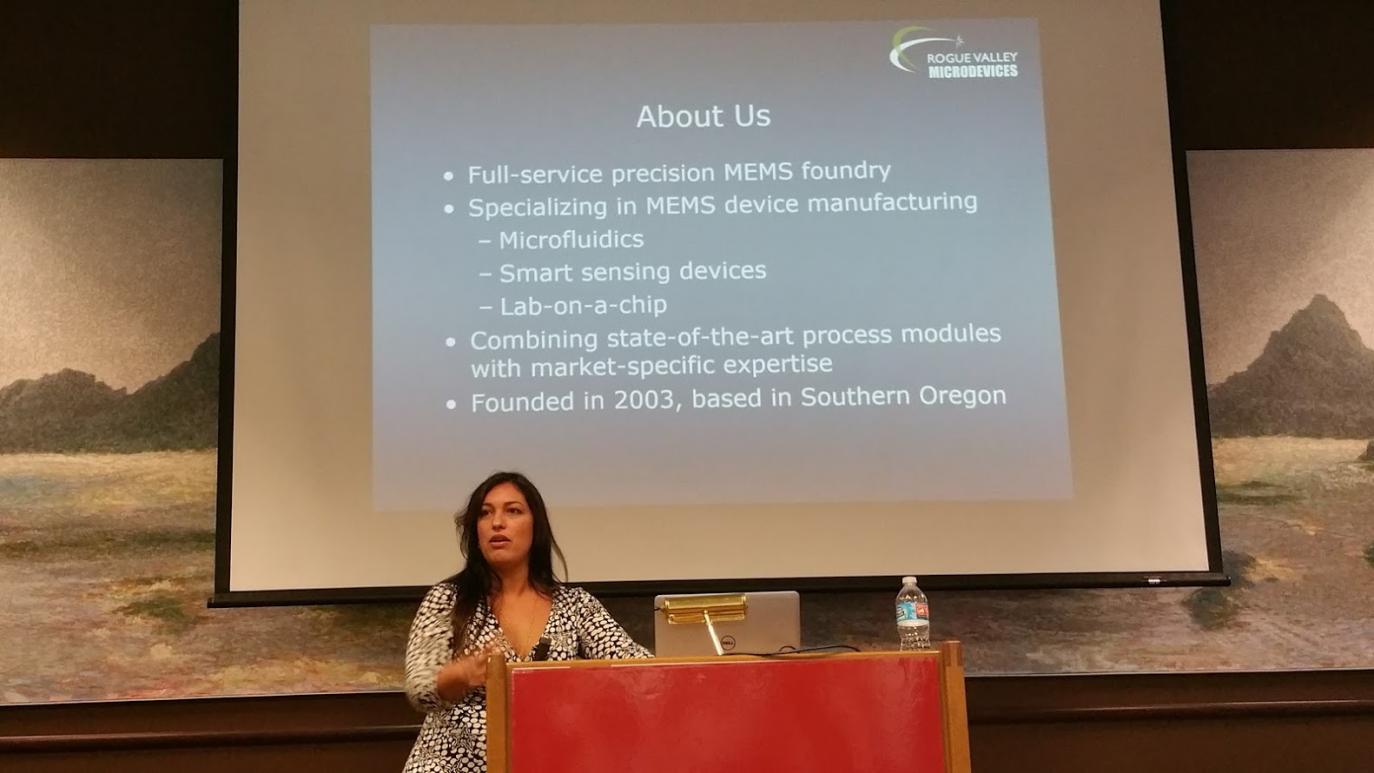
Rogue Valley Microdevices
I was surprised to learn that there’s a MEMS foundry in Medford, Oregon located south of Portland. Jessica Gomez is the Founder and CEO of the company and she talked about their full-service MEMS service to start-ups, universities and businesses. Example uses for sensors in IoT are:
- Smart Homes
- Infrastructure
- Agriculture
- Medical
The MEMS market is $12B in size as of 2015, predicted to grow to some $19B by 2021. MEMS customers cannot get what they are looking for by approaching a traditional silicon-centric foundry, so the concept of MEMS foundries has taken hold to meet the demand. There’s not really a a standard process for MEMS like there is for logic, memory, or SoC devices..


Comments
0 Replies to “IoT From SEMI Meeting: EDA, Image Sensors, MEMS”
You must register or log in to view/post comments.