
The arrival of optical computing has been predicted every year for the last fifteen years. As with any other technology backed by prolific research, lofty goals get dialed back as problems are identified. What emerges first is a set of use cases where the technology fits with practical, realizable implementations.
When it comes to photonics, the obvious use case is high bandwidth I/O channels. The ability to multiplex separate data channels in different wavelengths onto a single glass fiber has been the cornerstone of fiber optic communications for decades. These days, it’s not difficult at all to get that done with an SFP transceiver, a physical transition at the edge of a board from electrical to light domain. The idea in play now is to move that transition closer to the processing – and that has significant challenges.
Photons just work differently than electrons, and those differences drive layout and verification of photonic ICs. The photonic approach requires a combination of methods from traditional mixed signal design, RF design, high speed digital design, an understanding of the fab technology needed, plus light-domain expertise. That sounds scary, right? As the saying goes: if it were easy, everyone would do it. Fortunately, borrowing technology from those other design methodologies and adding knowledge of photonics is making some very cool things possible.
I’m struck by this quote in a new white paper co-written by a team at Luceda Photonics (a company started as a spin-off of imec) and the Tanner EDA experts at Mentor Graphics.
There is a large gap between what the silicon photonic technology can accomplish and the functionality that designers can actually design and simulate.
Several of the problems they point out are related to the waveguide nature of photonic design, forcing layouts into a single layer with very specific design and interconnect rules. Another area of big concern is the highly customized process design kits (PDKs) for photonic design, and the heavy burden placed on simulation due to the light spectrum frequencies and electromagnetic, electro-optical, and thermal parameters.

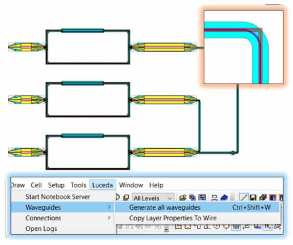
The goal is a design flow that moves from intense academic photonic knowledge to a production-ready environment that looks more familiar to designers coming from mixed signal backgrounds. Luceda Photonics has stepped in with their IPKISS.eda design framework built on Tanner L-Edit. This integration was made possible by use of the OpenAccess database standard and API, including heavy use of Python macros extending L-Edit functionality.
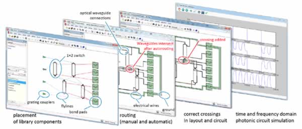
The white paper goes into detail with design of a 2×2 optical crossbar switch based on a Mach-Zehnder Interferometer thermo-optic switch. I’m not a photonic expert nor do I play one on TV, but I’ve done enough RF layout to appreciate how the Luceda environment handles waveguide generation. Note how the Luceda extensions appear as a new set of pull-downs in the familiar Tanner L-Edit tool:
Using Tanner Calibre One nmDRC, design rule checks can be run quickly using the rule deck from the photonic foundry, and highlighted in the results browser against the layout. Functional verification is performed with Luceda’s CAPHE optical circuit simulator. With the photonic environment fully integrated in IPKISS.eda, designers get help from automation with a large degree of control.
The complete white paper is available from Mentor Graphics (registration required):
Luceda Photonics Delivers a Silicon Photonics IC Solution in Tanner L-Edit
I remember the days of brute force RF and MEMS layout and funky tools that didn’t integrate with much of anything except a printer and a file the fab hopefully understood. This white paper is a good read on two fronts: how Luceda used open extensibility features to add functionality to L-Edit, and how challenging photonic chip design still is. I’m encouraged by the progress here. Certainly the philosophy Luceda is pursuing is correct – make photonic design as easy as advanced mixed-signal design. Leveraging Tanner’s capability not only got them there faster, it helps reduce EDA tool fragmentation and reduces the learning curve for users.
Making photonic design more straightforward should increase the number of photonic designs people will be willing to attempt, and that in turn should speed up overall innovation in the field.
Share this post via:


Comments
0 Replies to “Making photonic design more straightforward”
You must register or log in to view/post comments.