Waving white surrender flag as TSMC dominates-
The quarter was a success but the patient is dying-
Packaging now critical as Moore progress stumbles-
Intel reported a great quarter but weak H2 guidance-
But 7NM slip and “fab lite” talk sends shockwaves-
Intel reported a great quarter beating numbers all around with revenues of $19.7B and EPS of $1.23. Revenue was $1.2B better than expected and EPS was $0.13 better than expected. Guidance was for $18.2B and EPS of $1.10 as a widespread slowdown is expected to hit in H2.
Results for the quarter were great but other more significant issues far outweigh and swamp the quarterly results. We won’t waste time regurgitating the quarterly results which are well summarized in Intels slides:
Intel Earnings presentation
7NM products delayed at least 6 months while process is a year behind
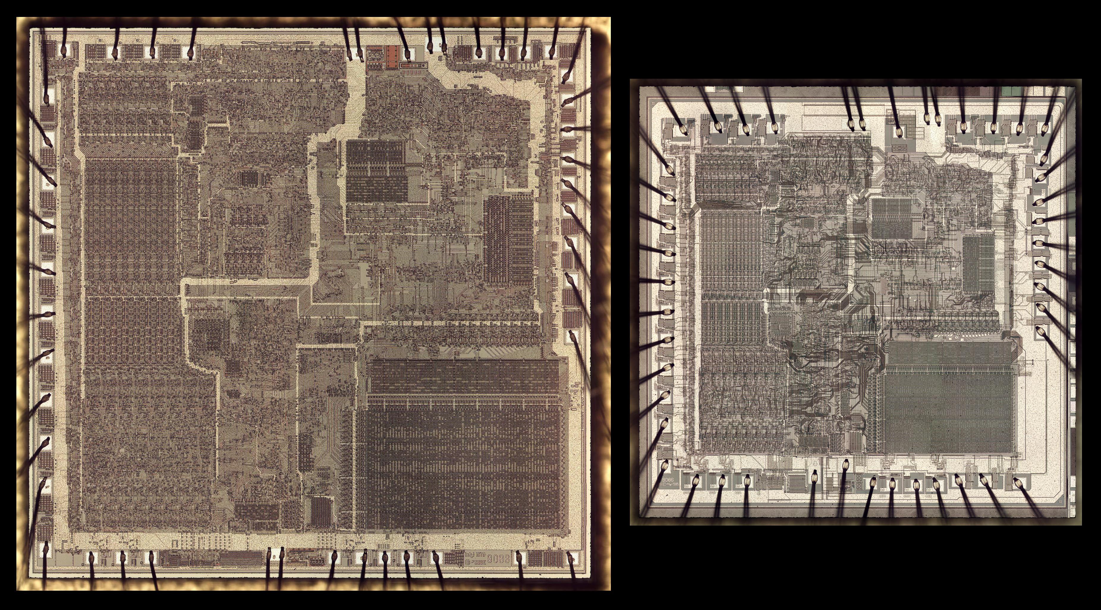
Echoes of the 10NM delay disaster. Perhaps the biggest news was that 7NM will be delayed at least another 6 months due to yield issues. This seems to put the overall 7NM delay at roughly a year. It was unclear wether this is “one and done” or if this is the beginning of another series of rolling delays as those that haunted 10NM. Either way the news is not good at all.
Rather than Intel regaining its “Mojo” as some had hoped at 7NM, to suffer another delay and fall further behind TSMC is just horrible, there is no way around it. Its a huge disappointment and heads will likely roll.
While management did suggest that the problem is understood and identified we came away without a firm feeling that it was under control, fixed or on its way to being fixed. Further slippage due to not finding a solution could easily happen as we saw at 10NM.
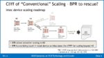
The 7NM slip is pushing Intel into a “fab lite” model following AMD’s lead-
Would make both Intel and AMD dependent upon TSMC…and more even-
During the earnings call, management made it quite clear that they are looking at alternatives for manufacturing of future nodes. Wether or not to outsource and how much to outsource to TSMC.
It seems from the tone of tonight’s call coupled with the 7NM slip that Intel is on the slippery slope to give more of its manufacturing to TSMC and perhaps TSMC will get to do Intel’s most leading edge manufacturing as Intel falls further behind.
Management couched it as a prudent allocation of resources and dollars but it sure sounds a lot more like waving the white flag of surrender after you’ve lost the race.
It sounds like sacrilege but Intel may be on the road to a “fab lite” model. Most semiconductor investors may not be old enough, but I can still hear the echoes of AMD’s founder, Jerry Sanders and his “real men have fabs” speech.
We can only hope that Intel can get its act together and get 7NM back on track and perhaps even make up some lost time, but we wouldn’t bet our investment dollars on it.
Intel joining Apple and AMD at TSMC’s fab on China’s doorstep…..
Apple obviously saw this coming and investors should have seen this coming with Apple’s recent announcement to give up on Intel. Apple correctly figured out that they could go straight to the source, TSMC, with their own customized design and do much better on their own
Obviously there will be little if any transistor density advantages between AMD and Intel if their advanced chips are built at the same TSMC fab. Differences will come down to design capability, which Intel continues to tout, but we don’t think there is that much there there.
The other ominous omen of Intel’s issues was likely the recent departure (for “personal reasons”) last month of Jim Keller, the famous CPU “Guru” who has had stints at AMD, Apple and Tesla designing their best CPU’s and who had joined Intel in 2018, with many hoping he could revamp things.
TSMC is obviously laughing all the way to the bank as Intel’s business will be huge upside, many times the size of Huawei business lost.
It would mean that in a couple of years, TSMC will be manufacturing every advanced chip on the planet. The demise of US chip making accelerates. We find the news of Intel going “fab lite” as a huge contradiction to the recent talk of the US governments “Chips for America” package of $22.8B in aid for the industry.
Intel’s talk of outsourcing to TSMC is in direct contradiction to Bob Swan’s personal lobbying of the White House and government officials and personal trips to DC to convince officials to have Intel lead a “trusted fab” initiative, while at the exact same time planning on outsourcing more manufacturing to TSMC .
It seems disingenuous to be lobbying to lead a US semiconductor resurgence initiative while at the same time calculating how much of the companies product to outsource to Taiwan.
The government should be highly embarrassed as Intel is the last advanced US semiconductor logic manufacturer after GloFo gave up the race. Micron is not the leader in memory. If the US government had any smarts they would match China’s $100B checkbook as well as push other efforts to keep manufacturing in the US.
TSMC’s “planned” fab in Arizona isn’t even throwing a bone to a dog as the capacity is far too little and far too far behind the leading edge to be of any consequence at all.
Packaging matters
One very interesting point that came out of the call will be Intel’s increasing reliance on advanced 3D packaging to mix and match heterogeneous die in a mixed package to optimize manufacturing and performance. Intel will be able to mix a 14NM die with a 22NM die, throw in a few memory dies into a heterogeneous package and increase Moore’s law without geometry shrinks which are obviously harder for them to do and increasingly delayed.
TSMC is already great at packaging and AMD has also pushed chiplet technology as well so unfortunately its not an advantage but just a “me too” technology for Intel.
The Stocks
Obviously Intel stock will get whacked as it did to the tune of 10% in the after market and perhaps even more so as the repercussions of the delay and outsourcing sink in.
The weak guidance doesn’t help but a weaker H2 is something we have been talking about for quite a while and the market should be expecting that. Perhaps there are still investors who think that the good times will continue into H2. Intel should be a wake up.
Intel guided capex to be $15B which is no surprise and the equipment stocks shouldn’t see much reaction from that but should likely see a negative reaction of the longer term negative out of Intel and increasing buying power of TSMC.
TSMC is looking at lot more like the old Intel with its dominance of capex spend in the industry. It is certainly not a positive for the US semiconductor industry to be so reliant on a tiny island “run away province”, soon to be re-united with mother China by any means necessary. All in all, not positive for the chip industry with perhaps the exception of TSMC and AMD.
Semiconductor Advisors
Semiconductor Advisors on SemiWiki

