You are currently viewing SemiWiki as a guest which gives you limited access to the site. To view blog comments and experience other SemiWiki features you must be a registered member. Registration is fast, simple, and absolutely free so please, join our community today!
When Analog FastSPICE was first introduced in 2006 it changed the landscape for high performance SPICE simulation. During the last 14 years it has been used widely to verify advanced nanometer designs. Of course, since then the most advanced designs have progressed significantly, making verification even more difficult. Just before DAC I had a conversation with Greg Curtis, Senior Product Manager at Mentor, a Siemens business, about these changes and Mentor’s newest improvements for Analog FastSPICE.
Greg pointed out three main drivers making verification more difficult. He said that the first is increasing interconnect resistance, which is jumping by a factor of 3 at nodes below 16nm. The second is increasing parasitic complexity. With more interconnect coupling and larger interconnect networks, the size of the RC networks is mushrooming. The final driver is new device models with large numbers of model equations – sometimes up to ~600.
While probably every tool during the last 14 years has benefited from improvements in performance, these changes hopefully have been enough to keep up. What designers are really looking for are manifold increases in performance – the kind that are game changing. This is especially true in the world of SPICE simulators, where the number of runs required has increased due to variation at the same time that complexity has increased.
Of course, design teams are used to EDA vendors rolling out new and improved versions of their software, but usually with a hefty price tag for the upgrade. Well, Greg was happy to inform me that on Monday July 20th Mentor is announcing Analog FastSPICE eXTreme with significant performance improvements at no additional cost for existing users. Availability is scheduled for October 2020. OK, but what do you get in this new version?
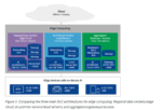
According to Greg, the focus of the improvements was on post layout simulation. It has become a reality that pre layout simulation is no longer useful, and the first real simulation is with parasitics. Mentor developed a new adaptive core SPICE matrix solver. They also enabled new RC reduction algorithms to help users meet performance and accuracy targets. The RC reduction operates with user-defined accuracy. As before Analog FastSPICE eXTreme will operate in the existing AFS Platform.
Greg had information showing the effectiveness of the speed up in Analog FastSPICE eXTreme. In the case of SRAM timing simulations times there was almost a 4X speed up. For a transceiver they boast a 15X speed up. A quick look at their data shows around an average speed up on various circuit types of 7X. These are impressive numbers.
Mentor was able to cite work with two early adopters on the results achieved with Analog FastSPICE eXTreme. Analog Bits, a leading provider of mixed signal IPs, such as PLLs, Sensors and IOs in processes down to 3nm, spoke of a 6X improvement in simulation times. Silicon Creations, developers of leading edge PLL and SerDes IP, also made comments supporting Analog FastSPICE eXTreme’s improved performance. They saw up to 10X improvement in simulation speed.
It is generally acknowledged that a 10X improvement in any design tool is meaningful in terms of getting users to switch tools. Mentor has taken their well-respected tool and given it that kind of performance improvement. Existing users should be delighted. Users of other tools are going to need to kick the tires simply out of necessity. The full announcement is available for review on the Mentor website. If you are doing SPICE on advanced process nodes, it will be well worth your while.
Semiconductor IP is one of the most talked about topics on SemiWiki. Always has been, always will be. Synopsys is also one of the most talked about topics on SemiWiki and IP is a very big part of that, absolutely.
After reading Eric Esteve’s latest IP Report I Googled around and found some interesting things. First, I found a Brief History of Synopsys DesignWare IP blog I did back in 2013. I also found the “Executive and Expert Access: Accelerating High-Performance Computing SoC Designs with Synopsys IP” webinar series and the DesignWare IP University (which I will be spending more time on in the coming days).
Don’t miss this opportunity to hear from Synopsys’ IP senior executives and product experts on how to accelerate your high-performance computing SoC designs. Find out about the latest market trends that will help you make important design decisions. Learn how specific features of Synopsys’ IP enables you to achieve the required functionality for your chip and deliver competitive products to market faster:
The New Frontier of Die-to-Die Connectivity: What You Need to Know for Silicon Success
Navigating Between DDR5, LPDDR5, and HBM2/2E IP to Meet Your Design Goals
Keys to Achieving Maximum Throughput and Lowest Latency for PCI Express 5.0 and CXL Designs
I just finished this on-demand webinar series. It’s easy to register and you get immediate access. The format is a 10 minute executive introduction, a 40 minute technical presentation, and a 10 minute Q&A, this is excellent content!
John Koeter is the Synopsys IP executive in the webinar series. John has been at Synopsys for more than 20 years and is one of the foremost semiconductor IP experts.
The Product Expert Speakers are:
Manmeet Walia brings over 18 years of experience in product management and system engineering covering ASSP, ASIC, and IP products for broad range of applications. Manmeet holds a Master of Science degree in Electrical Engineering from University of Toledo, and an MBA from San Diego State University.
Graham Allan brings over 25 years of experience in the memory industry. Graham has spoken at numerous industry conferences and is a significant contributor to the SDRAM, DDR and DDR2 JEDEC memory standards. He currently holds 25 issued patents in the area of memory design.
Gary Ruggles brings over 25 years of experience in electronics and integrated circuit design. Gary began his career as Assistant Professor of Electrical and Computer Engineering at North Carolina State University, where he taught courses in Solid State Physics and VLSI Processing.
This webinar series is definitely worth your time.
The DesignWare IP University is organized into 7 topics:
Interface IP
Processor IP
Foundation IP
Security IP
Artificial Intelligence
Automotive
Cloud Computing
Most of of these are trending topics on SemiWiki. Under each topic there are on-demand webinars, videos, event presentations, and white papers. This is an excellent resource that should be shared.
Learn about the latest interface protocols and standards, processor implementation techniques, and market trends in these educational white papers, webinars, and videos. Whether your chip design includes artificial intelligence capabilities, targets next-generation cars, or enables massive data in the cloud, the DesignWare IP University resources will help you create the SoC your market needs.
About DesignWare Synopsys is a leading provider of high-quality, silicon-proven IP solutions for SoC designs. The broad DesignWare IP portfolio includes logic libraries, embedded memories, embedded test, analog IP, wired and wireless interface IP, security IP, embedded processors and subsystems. To accelerate IP integration, software development, and silicon bring-up, Synopsys’ IP Accelerated initiative provides architecture design expertise, pre-verified and customizable IP subsystems, hardening, signal/power integrity analysis, and IP prototyping kits. Synopsys’ extensive investment in IP quality, comprehensive technical support and robust IP development methodology enables designers to reduce integration risk and accelerate time-to-market.
For those who design advanced and complex SoCs, the term “off-the-shelf IP” can be elusive. While this approach works for a wide range of IP titles, the pressure for maximum performance or minimum power can lead to custom-tailoring requirements for the IP.
PLDA has seen these requirements for the class of complex, high-performance IP the company is known for, such as PCIe 5.0 or CXL. Often, PLDA customers will require very specific features and configurations which trigger an IP modification cycle. In spite of this, each customer is expecting the delivered product to be proven, robust and reliable, as though it had been used in many prior tapeouts. This is a daunting requirement, but it’s the price of admission into the high-end IP market.
PLDA has developed a thoughtful and rigorous approach to this challenge. They’ve even developed an ecosystem to support their efforts – more on that later. I had the opportunity to get an overview of the work going on in IP verification from Romain Tourneau, Marketing Manager at PLDA.
Romain started with an overview of the spec requirements from the customer that need to be understood and managed. These include:
Functional requirements: behavior rules (this event is causing this consequence)
Parametric requirements: performance, gate count, power consumption
Structural/physical requirements: must be synthesizable, prone to metastability (CDC)
Aiming for a quality deliverable means requirements qualification to identify the “golden”, or most important items. Maximizing ways to verify these golden requirements then becomes the focus. This activity follows an implementation, debug and improvement process. There are many approaches to manage this process, including:
The standard approach (single process start to finish)
The incremental approach (following design changes incrementally)
The “Sprint” approach (the project is split into small, incremental releases)
The “Super-sprint” approach (same as Sprint, but accelerated timing)
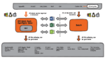
PLDA uses the Super-sprint approach, which is summarized below:
While there are still many manual and time-consuming tasks to perform, the iterative nature of the Super-sprint method allows for efficient collaboration with the customer. It requires a deep verification discussion with the customer at project kickoff in order to fulfill these objectives:
Understanding the customer’s process and tools
Know the customer’s verification plan and IP usage and associated cost
Explain PLDA process and tools
Identify gaps in design criteria and address possible solutions
Explain the advantages and importance of the customer starting IP verification early in their project since PLDA can provide a ready-to-use verification environment to perform this stand-alone verification earlier
You typically don’t often see such a proactive and broad approach to IP verification – this is noteworthy. The release states:
“The verification process for IP design takes place at the front end of chip design and requires a high level of reliability to prevent production delays. Achieving the necessary levels of verification can be time-consuming, however cutting corners in verification often results in costly and difficult bug fixes at the end of chip fabrication. It is much more efficient to ensure a robust and high-quality initial verification process.” This is a very informed and evolved point of view in my opinion.
Dubbed the Robust Verification Toolset, it includes:
Verification IPs covering standards compliance for PCIe, AMBA AXI, CXL, CCIX and Gen-Z
Simulators that support mixed-language designs with UVM testbenches
Synthesis and static verification tools from classic EDA providers, delivering verification of quality of RTL design and of CDC
To manage the data generated by the Robust Verification Toolset during both the verification and validation processes, PLDA has developed an interface named DANA.
This proprietary PLDA tool is used to deliver highly efficient supply chain management through a collection of automatic reports, flow automation and strict follow-up processes. Data from the complete toolset is automatically collected, analyzed, and reported. This reduces review cycles caused by data management and accelerates the decision-making process. A great gain of time for both projects leaders and verification engineers.
To learn more about PLDA’s verification solutions:
Many of us are now somewhat fluent in IoT-speak, though at times I have to wonder if I’m really up on the latest terminology. Between edge and extreme edge, fog and cloud, not to mention emerging hierarchies in radio access networks – how this all plays out is going to be an interesting game to watch. Ron Lowman, DesignWare IP Product Marketing Manager at Synopsys, recently released a technical bulletin which provides some quantified insight in the motivation of moving compute and AI closer to the edge, and how these changes affect IP selection and system architectures.
Hierarchy in radio access networks
The basics are well-understood by now, I think. Shipping zettabytes of data from billions or trillions of edge devices to the cloud was never going to happen – too expensive in power and bandwidth. So we start moving more of the compute closer to the edge. Handling more of the data locally, requiring only short hops. Ron cites one Rutgers/Inria study using a Microsoft HoloLens in an augmented reality (AR) application. This was tasked to do QR code recognition, scene segmentation and location and mapping. In each case the HoloLens first connects to an edge server. For one experiment, AI functions are shipped off to a cloud server. In a second experiment, these are performed on the edge server. Total roundtrip latency in the first case was 80-100ms or more. In the second case, only 2-10ms.
Not surprising, but the implications are important. The cloud latency is easily long enough to induce motion sickness in that AR user. In other applications it could be a problem for safety. The edge-compute round-trip latency is much less of a problem. Ron goes on to add that 5G offers use-cases which could drop latency under 1ms. Making the case for edge-based compute no contest. Going to the cloud is fine for latency-insensitive applications (as long as you don’t mind the cost overhead in all that transmission. And privacy concerns. But I digress.) For any real-time application, compute and AI has to sit close to the application.
Architectures from the cloud to the edge
Ron goes on to talk about three different architectures for edge computing, in a way I found novel. He sees edge as anything other than the cloud, drawing on use models and architectures from a number of sources. At the top end are regional data centers, somewhat more locally you have on premise servers (maybe in a factory or on a farm) and more locally still you have aggregators/gateways. Each with their own performance and power profiles.
Regional data centers are scaled-down clouds, with same capabilities but lower capacity and power demand. For on-premise servers, he cites an example of Chick-Fil-A who have these in the fast food outlets, to gather and process data for optimizing local kitchen operations.
The aggregators/gateways he sees performing quite limited functions. I get the higher-level steps in this architecture; however, I’ve seen this hierarchy go further, right down into the edge device, even battery-operated devices. In a voice-activated TV remote for example. I know of remotes in which voice activation and trigger word recognition happens inside the remote. Ron’s view still looks pretty good, maybe just need to add one more level. And possibly consider the gateway may do a bit more heavy lifting (command recognition for example).
He wraps up with a discussion on impact on SoC architectures and the IP that goes into server SoCs and AI accelerators. I agree with his point that the x86 vector neural network extensions probably aren’t going to make much of a dent. After all, Intel developed Nervana (and now Habana) for a reason. More generally, AI accelerator architectures are exploding. Very much in support of vertical applications, from the extreme edge to 5G infrastructure to the cloud. AI is finding its place throughout this regime, in every form of edge and non-edge compute.
Semiconductor technology advances have a way of rewriting the rule book. As process geometries shrink, subtle effects graduate to mainstream problems. Performance curves can become inverted. And no matter what else occurs, low power demands are constantly reducing voltage and design margins along with it. Sometimes these problems can be solved by just being more careful, and sometimes they require a new way of approaching the problem altogether.
I had an opportunity to explore the latter case recently. I spent some time with Brandon Bautz, senior product management group director and Hitendra Divecha, product management director in the Digital & Signoff Group at Cadence. Both of these gentlemen have been working on advanced chip designs for more than 20 years, so I was in good hands.
We discussed the new Cadence Tempus™ Power Integrity Solution, or Tempus PI, for short. Why is this so interesting and important? Winding back the clock a bit, Hitendra began by explaining that customers had reported max frequency failures in advanced node silicon. The problem manifested with up to 10 percent performance degradation. This translates to hundreds of megahertz out of spec, so it gets attention. Thanks to low power/low voltage operation requirements, you can’t margin your way out of this problem. There just isn’t enough margin. So, what’s causing these failures, and what’s the fix?
The root cause appeared to be related to localized IR drop, but there is a twist. As the process moved from 28nm to 7nm, conductor resistance through the power grids has increased by 10X. This means the traditional method of inserting decoupling capacitors to alleviate localized IR drop is no longer as effective. Also, the change in cell delay vs. voltage becomes much steeper at low voltages in advanced processes. This means a small IR drop will create a large change in timing. These effects are summarized in the diagram below.
Since timing and IR drop have a co-dependent relationship, the designer needs an automated method to simulate the design such that both timing and IR drop problems are simultaneously considered. A user-defined vector approach is difficult as enough vectors to find the problem will create huge runtimes. Random vector approaches create too many combinations as well. It’s a bit of “needle in a haystack” problem. Aggressor and victim nets also need to be considered if there is simultaneous switching and coupling.
We then talked about the architecture of the Cadence signoff tools, specifically how Tempus™ Timing Signoff Solution and Voltus™ IC Power Integrity Solution have been built on a common database and runtime model from the start. By adding additional analysis capabilities to the mix, including machine learning techniques for vectorless stimulus, Tempus PI delivers IR drop-aware STA signoff—that is, voltage analysis that is timing-aware, and timing analysis that is voltage-aware. Using resistance, power, IR-drop and timing data, Tempus PI’s algorithm can identify voltage sensitive paths and potential aggressors. The result is a well-thought-out approach as to what timing paths and aggressors need to be carefully analyzed—not just random activity—solving the “needle in a haystack” problem.
Using the Innovus™ implementation System, timing and IR-drop problems can even be fixed with the ECO flow. As we continued our discussion it became clear the integrated nature of the Cadence tool suite was paying big dividends when it comes to addressing new problems that require simultaneous views to sort out. The figure below summarizes the complete flow.
The Cadence folks shared some results for the ECO flow on a CPU core design:
Before: 1,334 IR-drop victims, 110.5 mV peak IR-drop voltage
After: 87 IR-drop victims, 81.9 mV peak IR-drop voltage
93% fewer victims, 26% less peak IR with no setup/hold degradation. Impressive.
We concluded our discussion with a few customer case studies. I’ll cite two here, and they’re both 7nm designs.
Case 1: An extensive set of activity vectors was used by the customer to perform IR drop analysis. Of the top ten IR drop paths, four were confirmed as top risks with Tempus PI, but Tempus PI found six other top paths that were missed by the vector approach.
Case 2: Tempus PI identified 2,092 critical paths that would have been missed by the customer’s traditional derating method.
At this point, I’m a believer. By making IR drop analysis timing-aware, the new challenges of advanced technology can indeed be tamed. If you’re seeing these kinds of challenges, you should talk to Cadence.
This has got to be one of the most interesting and disruptive EDA acquisitions I have seen in some time. Another one that comes to mind is Siemens acquiring Mentor Graphics. We have been covering EDA PLM companies since the start of SemiWiki and have worked with most of them. If I had to keep score I would say it’s about even but it was just a matter of time before one of them busted loose, absolutely.
The press release is included but first let’s take a look at the Perforce company history based on their Wikipedia page to better understand what this acquisition really means and we can do a Q&A in the comments section.
Perforce Software was founded in 1995 in Alameda, California by Christopher Seiwald, a software developer and computer science graduate from UC Berkeley. Its first product was also called Perforce, and was a version control system allowing companies to collaborate on large software projects by keeping track of changes to both the source code and binary files.
In June 2013, the company released Helix Swarm, a tool for developers working in different geographical areas to collaborate on code review.
In June 2014, the company released a version of its Perforce versioning engine, by then known as P4D, which supported concurrency, the ability of a program to run multiple parts concurrently.
In March 2015, the company renamed its product as Perforce Helix. In October, the company collaborated with GitLab to release GitSwarm, a software tool that combined git distributed workflow for developers with Perforce’s single code repository.
In February 2016, Seiwald sold the company to investment group Summit Partners. The company headquarters was relocated to Minneapolis. In November, Perforce announced the acquisition of Seapine Software, a provider of application lifecycle management (ALM) tools. Seapine’s TestTrack ALM software was rebranded as Helix ALM.
In September 2017, the company acquired Uppsala, Sweden-based Hansoft, a developer of Agile planning software. Also in September, Perforce announced it had acquired Finnish repository management services company Deveo. Deveo’s products were merged into Perforce’s Helix TeamHub, its first solo venture for Git-based development teams.
In January 2018, Summit Partners sold Perforce to private equity firm Clearlake Capital. In May, Perforce acquired UK-based Programming Research (PRQA), a static code analysis firm.
In December 2018, Perforce announced the acquisition of Perfecto, a market leader in cloud-based automated mobile and web application test software solutions.
In January 2019, Perforce announced the acquisition of Rogue Wave Software, a software company with a focus on development tools for high-performance computing.
In April 2019, private equity firm Francisco Partners acquired 50% of Perforce, becoming an equal partner with Clearlake Capital.
In July of 2020, Perforce announced the acquisition of San Francisco based Methodics.
Perforce Continues to Grow Platform Already Used by Top Semiconductor Companies
MINNEAPOLIS, SAN FRANCISCO, and SANTA MONICA, July 20, 2020 – Perforce Software, Inc. (“Perforce”), a provider of solutions to enterprise teams requiring productivity, visibility, and scale along the development lifecycle, backed by Clearlake Capital Group, L.P. (together with its affiliates, “Clearlake”) and Francisco Partners, today announced it has acquired Methodics Inc. (“Methodics”), a leading provider of intellectual property lifecycle management and traceability solutions for the enterprise. The addition of Methodics further distinguishes Perforce in the DevOps market as a solution provider uniquely addressing the needs of some of the largest technology teams in the world facing extreme scale, time to market, and quality imperatives. Terms were not disclosed.
Perforce and Methodics previously had a strategic partnership in place, providing a fully integrated solution to manage IP from design all the way through production and reuse in the semiconductor industry. Many of the world’s top semiconductor companies already leverage Perforce and Methodics for electronic design and data management.
“The semiconductor and embedded software design markets continue to expand, especially as they serve growing AI, automotive, cloud, and IoT markets,” said Mark Ties, Perforce CEO. “Together with Methodics, Perforce will enable these markets to drive faster time to market, higher quality, greater operational efficiency, and increased security and compliance at scale. We are also excited about the opportunity to extend this joint solution into gaming, automotive, and other industries.”
“The importance of collaboration between multisite and multi-geographic design teams continues to intensify. Methodics solutions enable critical collaboration while assuring full traceability and reuse of important design assets and their associated metadata,” said Simon Butler, Methodics CEO. “We are excited to join the Perforce team, and we are confident that this acquisition will enable us to meet the needs of the semiconductor and embedded systems markets, as well as gaming, automotive, and beyond.”
“Maxlinear has been using Perforce Helix and Methodics IP life cycle management solutions for the past few years to increase our productivity and introduce a IP reuse methodology at Maxlinear” said Paolo Miliozzi, Vice President, SoC Technology at MaxLinear. “We are looking forward to the solutions that the combined companies will be able to deliver to us moving forward as MaxLinear continues to grow.”
About Perforce
Perforce powers innovation at unrivaled scale. With a portfolio of scalable DevOps solutions, we help modern enterprises overcome complex product development challenges by improving productivity, visibility, and security throughout the product lifecycle. Our portfolio includes solutions for Agile planning & ALM, API management, automated mobile & web testing, embeddable analytics, open source support, repository management, static & dynamic code analysis, version control, and more. With over 20,000 customers, Perforce is trusted by the world’s leading brands to drive their business critical technology development. For more information, visit www.perforce.com.
About Methodics
Methodics is recognized as the premier provider of IP Lifecycle Management (IPLM) and traceability solutions for the Enterprise. Methodics’ customers benefit from the products’ ability to enable high-performance analog/mixed signal, digital, software, and SOC design collaboration across multi-site and multi-geographic design teams and to track the usage of their important design assets. The company is headquartered in San Francisco, California, and has additional offices and representatives in the U.S., Europe, Israel, China, Taiwan, and Korea. For more information, visit www.methodics.com.
About Clearlake
Clearlake is a leading private investment firm founded in 2006. With a sector-focused approach, the firm seeks to partner with world-class management teams by providing patient, long-term capital to dynamic businesses that can benefit from Clearlake’s operational improvement approach, O.P.S.® The firm’s core target sectors are technology, industrials, and consumer. Clearlake currently has approximately $24 billion of assets under management and its senior investment principals have led or co-led over 200 investments. More information is available at www.clearlake.com.
About Francisco Partners
Francisco Partners is a leading global private equity firm that specializes in investments in technology and technology-enabled businesses. Since its launch 20 years ago, Francisco Partners has raised more than $24 billion in committed capital and invested in more than 275 technology companies, making it one of the most active and longstanding investors in the technology industry. The firm invests in opportunities where its deep sectoral knowledge and operational expertise can help companies realize their full potential. For more information on Francisco Partners, please visit www.franciscopartners.com.
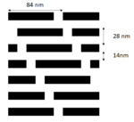
In the recent DRAM jargon, “1X”, “1Y”, “1Z”, etc. have been used to express all the sub-20 nm process generations. It is almost possible now to match them to real numbers which are roughly the half-pitch of the DRAM active area, such as 1X=18, 1Y ~ 17, etc. At this rate, 14 nm is somewhere around “1B”, and is some time away, maybe 2021 at earliest. Still, it is a good exercise to ponder the patterning possibilities of a 14 nm DRAM, using the representative pattern shown in Figure 1. Note that the layout is 6F2, which leaves too little distance between the transistor gates (9F2 would be more realistic [1]).
Figure 1. 14 nm half-pitch DRAM active area.
This pattern has some noteworthy symmetries. It repeats every six rows. Each row is also shifted by a sixth of a pitch. This greatly simplifies the diffraction pattern spectrum, consisting of plane waves exp[i*(m*2*pi*x/xpitch + n*2*pi*y/ypitch)], where m and n cover all integers. Only when m and n add up to a multiple of 6 will the plane waves be non-vanishing (see Appendix for proof).
Single EUV exposure
Of course, with the availability of EUV tools, single exposure using EUV is the first considered option. The possible diffraction patterns from Figure 1 for all the points in the pupil are shown in Figure 2.
Figure 2. Diffraction patterns for the pattern of Figure 1, originating from all possible different directions of illumination [2].
The radial distance here represents the sine of the illumination angle (multiplied by the system magnification of 4). The largest distance corresponds to the numerical aperture (NA) of 0.33, which is the upper limit for any angle. The points with radial distance up to 30% NA cannot resolve the individual horizontal rows, while the remaining pupil area includes altogether ~30 diffraction patterns, each taking its share of the photon dose. Assuming a 30 mJ/cm2 dose gives an average of ~1 mJ/cm2 per diffraction pattern. This gives less than one photon per square nanometer for each diffraction pattern, a very noisy image indeed! An average of ~3% pupil fill per diffraction pattern makes pupil fill a concern for throughput [3] unless several patterns are included, forcing us to walk back this only way to address the photon division problem.
EUV 28 nm pitch lines
It’s quite straightforward to find an optimum EUV source pattern for 28 nm pitch, which requires only two diffraction orders (0th and 1st). Figure 3 shows all the points which give at most 30 degrees phase shift between the 0th and 1st orders at 30 nm defocus.
However, due to rotation across the field [4], a rotation of 18 degrees already misplaces more than 20% of the source points, leading to a noticeable change in the image (Figure 4).
Figure 4. Dipole rotation effect across field significantly affects the 28 nm pitch image.
SAQP with cuts
Due to the fundamental issues of using EUV for the 28 nm pitch active area pattern shown above, self-aligned quadruple pattern (SAQP) starting with immersion lithography would have to be used. Since the SAQP is to produce regular lines in an array, the process flow is straightforward but care must always be taken to suppress or minimize pitch walking [5].
The cuts for the lines may be trickier, although they offer tighter line end gaps. Perhaps a single diagonal cut line (which can be done by immersion lithography) across all rows is tolerable without shaving too much of the line ends of the active area. Otherwise, a self-aligned cut process in DUV is preferred to EUV, due to overlay and stochastic concerns [5-7].
Summary of approaches
The 28 nm pitch DRAM active area patterning approaches covered above are summarized below:
Appendix: Vanishing diffraction orders in staggered arrays
A periodic function f(x) can be represented as a Fourier series, with x normalized to pitch:
In two dimensions, we can proceed similarly, normalizing both x and y with respect to x-pitch and y-pitch, respectively:
Each coefficient cmn is obtained through an integral:
For the staggered array of Figure 1, f(x) can be defined for different ranges of y, within the y-pitch, as follows:
f(x,y) = 1, 0<x<1/6, 0<y<1/6, (sub-pitch row 0)
1/6<x<2/6, 1/6<y<2/6, (sub-pitch row 1)
2/6<x<3/6, 2/6<y<3/6, (sub-pitch row 2)
3/6<x<4/6, 3/6<y<4/6, (sub-pitch row 3)
4/6<x<5/6, 4/6<y<5/6, (sub-pitch row 4)
5/6<x<1, 5/6<y<1 (sub-pitch row 5)
0, elsewhere
The integral for cmn for the jth row has the similar expression:
which is equal to sin(pi*m/6)/(pi*m)*sin(pi*n/6)/(pi*n)*exp[-ipi*m/6]exp[-ipi*n/6] exp[-i2pi*j(m+n)]/6]. For the special case m equal to 0, the sin(pi*m/6)/(pi*m) is replaced by 1/6.
Since this is for the jth row, the final value of cmn requires a sum from j=0 to j=5. When m+n is an integral multiple of 6, exp[-i2pi*j(m+n)]/6] = 1, so the sum adds up to 6, but when m+n is an integer that is not a multiple of 6, the sum in fact adds up to 0. This is because in this case 2pi(m+n)/6 represents a rotation going 1/6, 2/6, 3/6, … of the way around a circle, and adding 6 such consecutive rotations always gets you back to where you started; zero distance is traveled. The picture is consistent with the previous case with exp[-i2pi*j(m+n)]/6] = 1 as it can be understood as adding 6 unit vectors in a row, so the final distance traveled is 6.
So, for the staggered array of Figure 1, we see that cmn is 0 unless m+n is a multiple of 6.
References
[1] K. Lee, D. Kim, C. Yoon, T. Park, S. Han, Y. Hwang, K. Lee, H. Kang, H. Kim, “Self-aligned double patterning for active trim contacts with anisotropic pattern pitches in sub-20 nm dynamic random access memories,” J. Microlith/Nanolith. MEMS MOEMS 18, 040501 (2019).
[3] M. van de Kerkhof, H. Jasper, L. Levasier, R. Peeters, R. van Es, J-W. Bosker, A. Zdravkov, E. Lenderink, F. Evangelista, P. Broman, B. Bilski, T. Last, “Enabling sub-10nm node lithography: presenting the NXE:3400B EUV scanner,” Proc. SPIE 10143, 101430D (2017).
[4] S-S. Yu, A. Yen, S-H. Chang, C-T. Shih, Y-C. Lu, J. Hu, T. Wu, “On the Extensibility of Extreme-UV Lithography,” Proc. SPIE 7969, 79693A (2011).
[6] U. S. Patent 10,115,726, assigned to Tokyo Electron Ltd.
[7] A. Raley, N. Mohanty, X. Sun, R. A. Farrell, J. T. Smith, A. Ko, A. W. Metz, P. Biolsi, A. Devilliers, “Self-Aligned Blocking Integration Demonstration for Critical sub 40nm pitch Mx Level Patterning,” Proc. SPIE 10149, 101490O (2017).
Although much of the EDA industry has consolidated into the “Big 3” players, there are still plenty of smaller vendors in the market. In the earlier days of EDA, it seemed that most startups existed only until they failed or did well enough to be acquired. The industry has changed; there are now a number of notable companies that have existed independently for years, growing and thriving. Maybe they’ll be acquired someday, or maybe they’ll go public when times are better, but for now they’re doing just fine on their own. Agnisys is one of these successful companies, and to learn more about them I had a chat with CEO and founder Anupam Bakshi.
Who is Agnisys?
We’re an EDA company dedicated to solving complex design and verification problems for system development. We believe in a specification-driven development flow for registers and sequences in system-on-chip (SoC) and IP projects, and our products enable this flow. Our goal is to enable faster design, verification, firmware creation, and validation. Our products increase the productivity of individual engineers and projects teams, while producing better designs and verification environments by eliminating common errors.
What is your background?
I received both a BSc Electronics and an MSc Electronics from Delhi University in India. My early career focused on EDA, developing internal tools for several companies and working at Gateway Design Automation, the creator of Verilog, and Cadence. Along the way, I earned an MS in Computer Engineering and a High-Tech MBA from Northeastern University. I did some consulting work and led a verification team at Avid Technology before the entrepreneurial bug bit me and I founded Agnisys. That was in 2007, and we just celebrated our thirteenth anniversary as an independent company. It’s been a fun and challenging journey!
What customer issues do you address?
I started Agnisys to help solve some of the problems I faced first-hand in my previous roles. Chips keep getting bigger, and verification gets even harder. The only way for engineers to tackle this growth is to automate more of their development process. We started with IDesignSpec™ (IDS), which enables engineers to create an executable specification for registers and automatically generate outputs for software and hardware teams. The input specification can be in an industry-standard format such as SystemRDL or IP-XACT, or it can be created interactively by using a plug-in for Microsoft Word or Excel. IDS produces all sorts of outputs, including synthesizable Verilog and VHDL RTL, UVM models, C, Word, HTML, and other formats. Automatic generation saves project engineers weeks or months of time while eliminating the inevitable errors in hand-written code.
Are you an IP company as well as an EDA vendor?
That’s a really good point. We usually don’t describe ourselves that way, but we do generate IP. The RTL becomes part of the chip design, the UVM models become part of the testbench, the C headers are used in diagnostic and device driver programs, and the Word and HTML files are incorporated into the chip documentation.
Do you have other products available?
We have extended register automation in two major directions. Automatic Register Verification (ARV™) is an add-on to IDesignSpec for automatically verifying and validating all registers, including complex types. ARV generates the complete UVM testbench: bus agents, monitors, drivers, adaptors, predictors, sequencers, and sequences, plus a makefile and a verification plan. It generates assertions for formal tools. It can also generate tests for a variety of platforms including bare-metal hybrid C-UVM platforms. The generated files support both popular industry simulators and formal verification tools.
We have also expanded beyond registers to generate sequences for IP blocks such as bus interfaces. ISequenceSpec™ (ISS) enables users to describe the configuration, programming, and test sequences of an IP and automatically generate programming and test sequences ready to use. ISS generates UVM sequences for verification, C code for firmware and device driver development, CSV for Automatic Test Equipment (ATE) post-silicon validation, and more.
What’s new at Agnisys?
There’s a lot new, actually. At this year’s virtual Design Automation Conference (DAC), we announced general availability of three major new products that have been in development and use by early adopters for some time. You pointed out that we are also an IP provider, and we’ve moved more in this direction with our new SLIP-G™ (Standard Library of IP Generators). We offer an interface for IP customization and configuration, and generate the design RTL, the UVM testbench models, and the programming sequences. We have GPIO, I2C, timer, and programmable interrupt controller (PIC) IP available today, and we expect the library to grow over time based upon customer demand.
Assembling the SLIP-G IP and other blocks into an SoC is a huge challenge. Chips may have 500 or more major blocks and tens of thousands of connections among them. We developed SoC Enterprise™ (SoC-E) to be a flexible and customizable environment for design assembly of the most complex chips. We have made even more IP available; SoC-E can generate RTL aggregators, bridges, and multiplexors as needed by the SoC architecture. SoC-E’s Smart Assembler technology automatically integrates and connects these blocks, SLIP-G IP, IP from other sources, and user blocks into a complete SoC.
Finally, at DAC we announced IDS NextGen™ (IDS-NG), a specialized integrated development environment (IDE) for large IP blocks and SoCs. It provides a sophisticated GUI for capturing register and sequence specifications. We’ve made it available on Windows, Linux, and MAC platforms for maximum usability. It serves as a common front end for IDS, ARV, ISS, and SoC-E, enabling the fully automated flow of registers and sequences that we’ve envisioned for years. IDS-NG will help all users increase their efficiency, improve their design and verification quality, reduce project costs, and minimize time to market.
I read that Agnisys has taken the Open COVID Pledge; what is that?
We have joined a group of companies who have pledged free IP to help fight the deadly pandemic. Specifically, we make our tools and generated IP available for free to any engineers designing chips for medical applications in the research, diagnosis, or treatment of COVID-19. We really hope that we can help enable some real solutions.
Where are you located and who are your customers?
We’re headquartered in Boston, Massachusetts, with R&D centers and application engineers in the United States and India. Agnisys is a privately held company, self-funded and profitable thanks to the quality of our products and our outstanding customer service. We have customers located around the world, with a partial list at https://www.agnisys.com/agnisys-customer/.
Results were in line after correcting Covid Caused Revenue Rec issue-
ASML reported revenues of Euro3.3B and EPS of Euro1.79 as revenues from two EUV systems was not recognized, due to Covid related issues and delays, causing the miss. Had the systems been recognized, revenues would have been in line with expectations of Euro3.6B and EPS obviously would have been more in line as well
Guidance for Q3 is revenues between Euro3.6B and Euro3.8B which may be a liitle less than what was otherwise hoped for but still in reasonably good shape despite the Covid Crisis.
Order drop is more concerning
After having a string of strong order quarters, orders dropped in the second quarter to Euro1.1B, or less than a third of sales reflecting a very low book to bill ratio. Perhaps even more concerning was that only 3 EUV tools were ordered in the quarter accounting for Euro461M of the orders
We had reported several weeks ago about TSMC pushing out equipment orders and the drop in orders could be partially due to this. Orders were roughly balanced between memory and logic but perhaps more due to logic falling off more than memory gains as the overall number was very low.
The order fall off is likely due to a number of factors but uncertainty about the economic outlook due to Covid related issues is clearly the chief concern. We have been talking about an H2 fall off since the beginning of the Covid Crisis as we expected the trickle down impact economic to extend into the fall.
Given that litho tools are the last thing that a fab wants to cancel due to the very long lead times, this could have a more ominous impact on other tools, such as dep and etch which are more of a turns business and could more easily be canceled or pushed out than litho tools
Could we be seeing EUV “digestion” or pause as well?
Aside from the obvious Covid and economic concerns we could also potentially be experiencing a digestion period for the slew of EUV tools that were ordered and shipped as EUV turned into an HVM tool set.
Now that many fabs are in production perhaps we are also seeing a pause or digestion of the first round of EUV tools that everyone implemented into their process flow.
In any event, backlog is a wonderful thing, as it helps smooth out the ebbs and flows and lumpiness of orders of big ticket items. ASML has a very strong order book/backlog looking at 54 systems which helps keep production and revenues more steady even though it may not prevent revenue recognition hiccups.
Other long lead time tools makers such as KLA also have the luxury of long order books smoothing out a lumpy, seasonal, cyclical business. We would not be surprised to see order drop offs from other tool makers as we approach H2
Long term picture and EUV technology remain very much on track
Despite the revenue miss and order drop, we see no change in the dynamics of EUV adoption and technology advancement. ASML also announced a new dry DUV tool in the quarter as well as shipping their first multi beam wafer inspection tool obviously aimed at KLA.
Further improvements and refinements of EUV source technology were evident with the tin refill capability discussed. The company is also pioneering an augmented reality service tool to help deal with Covid 19 service issues we have detailed in the past
The Stocks
As we would expect, ASML’s stock will be down due to a combination of the financial miss coupled with the weak order book which portends the uncertainty of the market. Other semiconductor equipment stocks will likely be weaker in anticipation of similar cause for concern in H2 business and potentially worsening business environment for chip equipment.
We wouldn’t lose all that much sleep as the valuations of these semiconductor equipment names and other semi names have been on fire with valuation multiples reaching all time highs despite an ugly economic environment fraught with uncertainty.
We could see more air come out of high flying semi stock valuations as quarterly reports will not reflect the stocks strong performances.
This is going to be a record setting year for DAC content and attendance, absolutely!
My first DAC was in 1984 in Albuquerque New Mexico, right out of College, and I married my beautiful wife two months later. Thirty six DAC’s later I have four grown children, grandchildren, and the number one semiconductor design portal in the world. What an amazing ride!
This year however will be one for the record books. 57th DAC has gone virtual enabling a world wide conference experience. Due to the pandemic SemiWiki activity has increased dramatically which is a good sign for virtual conferences. Semiconductor professionals are now online more than ever before and the surge continues. The question is: Will we go back to live conferences in 2021? One of the biggest arguments for live events is the networking. It will be interesting to see how the virtual networking goes next week. We can better answer that question in our post DAC coverage.
So without further ado, here is my DAC must see list:
Wally is the best speaker EDA will ever have so you don’t want to miss this one. It’s in the DAC Pavilion. I got a sneak preview and it does not disappoint.
Cloud Talks: There is quite a bit of cloud content again this year but honestly I’m tired of talking about it. Just do it already. If you are not designing chips in the cloud like Google, Amazon, Facebook, Huawei, Apple, and the other A list system companies we will be seeing you in the rearview mirror.
The virtual DAC booths are up now and here are the ones I know personally and professionally (alphabetically). The big value here is the chat and private meetings in my opinion. Some of the booths have CEOs available for chats so you do not want to miss that networking opportunity:
Aldec: Chat with Louie De Luna (10+ years with Aldec)
Established in 1984, Aldec is an industry leader in Electronic Design Verification for SoCs/ASICs and FPGAs and offers a patented technology suite in the areas of RTL Design and Mixed-Language Simulation, FPGA-based Emulation and Prototyping with multi-FPGA partitioning, Design Rule Checking, Clock Domain Crossing, VIP Transactors, Requirements Lifecycle Management, Embedded Development Kits, High-Performance Computing/Acceleration, DO-254 Functional Verification and Military/Aerospace solutions.
Agnisys: Chat with CEO Anupam Bakshi
Agnisys Inc. is a leading supplier of EDA software for solving complex design and verification problems in system development. Our products provide a common specification-driven development flow to describe registers and sequences for SoC and IP projects, enabling faster design, verification, firmware creation, and validation. Based on patented technology and intuitive user interfaces, our products increase productivity, efficiency, and work quality of individual engineers and project teams, while eliminating system design and verification errors.
Altair: Chat with Long time EDA professional Jim Cantele
Altair is a global technology company that provides software and cloud solutions in the areas of product development, high performance computing (HPC) and data analytics. Altair enables organizations across broad industry segments to compete more effectively in a connected world while creating a more sustainable future.
AMIQ EDA:Chat with CEO Cristian Amitroaie
AMIQ EDA provides tools – DVT Eclipse IDE, DVT Debugger Add-On, Verissimo Linter, and Specador Documentation Generator – that enable design and verification engineers to increase the speed and quality of new code development, simplify legacy code maintenance, accelerate language and methodology learning, and improve source code reliability. Working with 100+ companies in 30+ countries, AMIQ EDA is recognized for its high quality products and customer service responsiveness.
ANSYS: Chat with EDA long time professional Marc Swinnen.
As the global leader in engineering simulation, Ansys Semiconductor solutions are the industry’s leading provider of power integrity, thermal analysis, and reliability software for chip designers across all market sectors – from ultra-high speed radio frequency designs for 5G to the world’s advanced processors for autonomous vehicles, HPC, AI and more.
Breker Verification Systems:Chat with CEO Adnan Hamid.
Breker’s Test Suite Synthesis accelerates and simplifies the production of verification test content for UVM, SoC and Post-Silicon environments. In use across the semiconductor industry, customers have seen a 5X acceleration in content production time, with equally dramatic improvements in coverage.
Circuitsutra Technologies: Chat with CEO Umesh Sisodia.
CircuitSutra is an Electronics System Level (ESL) design IP and services company, headquartered in India, having its offices at Noida, Bangalore and Santa Clara (USA). It enables customers to adopt advanced methodologies based on C, C++, SystemC, TLM, IP-XACT, UVM-SystemC. Its core competencies include Virtual Prototype (development, verification, deployment), High-Level Synthesis, Architecture & Performance modeling, SoC and System-level co-design and co-verification. CircuitSutra is developing modelling infrastructure for the RISC-V ecosystem.
Cliosoft: Chat with EDA and IP professional Simon Rance.
Concept Engineering: Chat with CEO Gerhard Angst
Established in 1990, we are celebrating 30 years of innovations in 2020. Concept Engineering is the leader in electronic system visualization software, with applications in multiple industries. We help engineers debug complex semiconductor designs, and provide powerful OEM visualization engines to computer aided tool developers for their EDA product lines.
Defacto:Chat with CEO Chouki Aktouf.
Defacto Technologies is an innovative chip design software company providing breakthrough RTL platforms to enhance integration, verification and Signoff of IP cores and System on Chips. This year we are announcing the latest release of our RTL Design Platform: STAR 8.5. In conjunction with new customer success stories in SoC Integration areas including UPF promotion and demotion, support of RTL<->IPXACT translation and many other new capabilities our experts will provide live presentations on a dedicated Zoom.
Empyrean Software: Chat with CEO Jason Xing
Empyrean Software is an EDA and service provider, serving fabless semiconductor design houses and IDMs throughout Asia, North America and Europe with unique and best in class design solutions. Our President / CEO of North America, Jason Xing, prepared a short video on our offering in this year’s DAC. Also you will find ALPS-GT and Skipper intro videos.
Fractal Technologies: Chat with CEO Rene Donkers
since 2010 Fractal has been solely dedicated to providing comprehensive design and technology agnostic solutions to enable its customers and partners to validate the quality of internal and external IPs. Thanks to its validation solutions and worldwide support, Fractal Technologies maximize value for its customers either at the sign-off stage, for incoming inspection or on a regression testing fashion within the design flow process. Come and see Fractal Crossfire and IPDelta.
GLOBALFOUNDRIES: Chat with the GF foundry staff.
GLOBALFOUNDRIES (GF) is the world’s leading specialty foundry. We deliver differentiated feature-rich solutions that enable our clients to develop innovative products for high-growth market segments. GF provides a broad range of platforms and features with a unique mix of design, development and fabrication services. With an at-scale manufacturing footprint spanning the U.S., Europe and Asia, GF has the flexibility and agility to meet the dynamic needs of clients across the globe. GF is owned by Mubadala Investment Company. For more information, visit globalfoundries.com
Intento Design: Chat with EDA and IP professional Daniel Borgraeve.
Intento Design develops analog EDA to eliminate the productivity gap inherent to the analog design process and empower our customers in achieving FIRST-TIME-RIGHT analog IP design in drastically less time.
Magwell: Chat with CEO Dundar Dumlugol
Magwel® offers 3D solver and simulation based analysis and design solutions for digital, analog/mixed-signal, power management, automotive, and RF semiconductors. Magwel software products address power device design with Rdson extraction and electro-migration analysis, ESD protection network simulation/analysis, latch-up analysis and power distribution network integrity with EMIR and thermal analysis.
Menta: Chat with Managing Director Yoan Dupret
For ASIC and SoCs designers who need fast, right-the-first time design and fast time to volume, Menta is the proven eFPGA pioneer whose design-adaptive standard cells based architecture and state-of-the-art tool set provides the highest degree of design customization, best-in-class testability and fastest time-to-volume for SoC design targeting any production node at any foundry.
Mentor @ DAC Conference Overview – 3 papers – 8 posters – Several videos covering Mentor news from DAC – Booth Visitors receive a $5 Starbucks gift card. Main Booth and Cloud Booth.
Methodics: Chat with Michael Munsey (30+ year EDA professional)
Methodics is recognized as the premier provider of IP Lifecycle Management (IPLM) and traceability solutions for the Enterprise, including Functional Safety and IP security assurance. Methodics solutions enable high-performance hierarchical analog/mixed signal, digital, software, embedded software, and SOC design collaboration across multi-site and multi-geographic design teams, assuring full traceability of the use and reuse of important design assets for Functional Safety compliance with such standards as ISO26262 and DO-254.
Mixel: Chat with CEO Ashraf Takla.
Mixel is a leading provider of mixed-signal IPs and offers a wide portfolio of high-performance mixed-signal connectivity IP solutions. Mixel’s mixed-signal portfolio includes PHYs and SerDes, such as MIPI D-PHY(SM), MIPI M-PHY®, MIPI C-PHY(SM), LVDS, and many dual mode PHY supporting multiple standards. Mixel was founded in 1998 and is headquartered in San Jose, CA, with global operation to support a worldwide customer base.
NetApp: Chat with long time EDA professional Scott Jacobson.
The cloud is clearly the next phase of development for modern EDA workflow design. Traditional EDA workflows are being strained to support the levels of compute and storage leading edge process technologies like 10nm, 7nm and 5nm require. This is placing a heavier burden on IT infrastructures than traditional on premises solutions can bear. When organizations take advantage of cloud elasticity they can operate EDA workflows at lower costs when not busy and rapidly scale when more resources are needed. This is why, as EDA vendors, designers, and semiconductor manufacturers develop more integrated workflows, the cloud will be the next logical phase of integration and NetApp solutions are there to make this journey successful.
Semifore: Chat with CEO Rich Weber.
Semifore generates the hardware/software interface (HSI) for SoC designs, including the synthesizable RTL, documentation and testbench. We read available specification languages to gather design intent and output the formats needed for all stakeholders, unifying the entire design team around one robust and well-documented HSI. Semifore builds the foundation layer for SoCs that run software, allowing the design team to focus on architectural innovation with the confidence that the HSI will support their breakthroughs.
SmartDV: Chat with the SmartDV staff.
SmartDV Technologies is the Proven and Trusted choice for Verification Intellectual Property (VIP) and Design IP. SmartDV offers the largest portfolio of high-quality standard or custom protocol VIP compatible with all verification languages, platforms and methodologies supporting simulation, emulation, FPGA, formal verification, and post-silicon validation platforms tools used in a coverage-driven verification flow.
Synopsys: Chat with the Synopsys staff.
Synopsys technology is at the heart of innovations that are changing the way people work and play. Self-driving cars. Machines that learn. Lightning-fast communication across billions of devices in the datasphere. These breakthroughs are ushering in the era of Smart Everything where devices are getting smarter, everything is connected, and everything must be secure. Powering this new era of digital innovation are high-performance silicon chips and exponentially growing amounts of software content. Synopsys is at the forefront of Smart Everything with the world’s most advanced technologies for chip design, verification, IP integration, and software security and quality testing. We help our customers innovate from silicon to software so they can bring Smart Everything to life.
Tortuga Logic: Chat with CEO Jason Oberg
Recently hackers have been targeting the heart of our most complex systems, the FPGAs, ASICs and SoCs that run and control them. Tortuga Logic, founded in 2014, specializes in hardware security solutions and services. Our Radix solution provides advanced analysis that helps security and verification teams identify and isolate security vulnerabilities before the device is manufactured, saving costly design re-spins or catastrophic system failure due to an attack. Radix has been developed to fit seamlessly into existing design and verification tools and methodologies protecting your current verification investment.