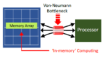
Bronco Webinar 800x100 1

High Speed SerDes Design and Simulation Webinar Replay from Mentor

High Speed SerDes Design and Simulation Webinar Replay from Mentor
by Tom Simon on 05-14-2020 at 10:00 am

Mentor SerDes Simulation

Over the years SerDes (serializer/deserializer) based connections have proliferated into just about every connection within and among computing systems. Years ago, parallel interfaces were the most common method of moving data, but issues of signal integrity, synchronization and power simply became too much for the required data rates. One by one old parallel links have been updated to modern serial connections. Remember parallel printer cables, ATA & IDE, or PCI connectors, to name a few? These have all been updated to serial equivalents and even on-chip connections between blocks have adopted network on chip architectures that rely on high speed serial links for moving packetized data.

The new age of USB, PCIe, NoC, ever faster memory, network and device interfaces have pushed SerDes designs into challenging high-speed realms. A single serial link carrying what used to be carried by a set of parallel wires needs to run that much faster. Add to it packetization, error correction and encoding and the speed requirements for SerDes become substantial.

All of these factors have made SerDes design critical for every market, including networking, IoT, automotive, servers, etc. One of the biggest challenges is verification with simulation. Modern SerDes have a mixture of digital and analog, thus making it impractical to run analog and/or digital simulation independently. Mentor, a Siemens Business, has recorded a webinar that breaks down the issues and potential solutions for SerDes simulation. In the video titled “Addressing Analog Mixed-Signal Verification Challenges of High Speed SerDes”, Scott Guyton, Solution Architect Manager in the Mentor AMS BU discusses all the facets of this issue.

Scott begins by summarizing the need for widely deployed high speed SerDes throughout electronic products. As mentioned above, all the major markets need increasing rates of data transfer and processing power. Some of the design challenges for these systems are clock and data recovery, dealing with high db loss & crosstalk, low power operation and support for multiple current and legacy protocols. Scott talks about how these system level challenges translate into SerDes circuit design challenges. High data rates call for stringent jitter and phase noise requirements. High channel loss necessitates equalization architectures and increased design complexities.

SerDes are not immune to issues found in advanced nodes. Long gone are the days where an interface SerDes could stay on an older process while the core moved to a new node for performance or capacity. SerDes designs also have to wrestle with clock domain crossings, programmable parameters and complex data paths. All of this this must be done while maintaining tight design margins.

Mentor has assembled a comprehensive simulation solution that addresses the digital, analog and mixed signal domains needed for SerDes design. Scott reviews the requirements in the webinar. He divides them up into Performance, Accuracy, Capacity and Ease of Use (PACE). Analog simulation is used for transient, transient noise and RF. Mixed signal needs to maintain SPICE accuracy and allow for sufficient cycles of digital or channel model to validate the design. Digital simulation covers corners and Monte Carlo to assure yield and help with design optimization.

Mentor offers their Symphony Mixed Signal Platform, which is powered by AFS and can integrate with a wide range of industry standard HDL simulators. Symphony lets designers switch between analog, digital and behavioral models to trade off performance or accuracy, as needed. With AFS, runtimes are dramatically shortened to allow more simulations in a smaller period of time.

Scott closes the webinar with a set of case studies showing how their customers took advantage of the Mentor simulation platform. The first case study includes information on simulation accuracy versus measured silicon at 7nm for SerDes intended for automotive and IoT applications. The second case study is a specially designed SerDes for use in a GPU interface PHY. The customer was able to run a mixed signal simulation at high accuracy with fast runtimes using Symphony. The third case study was a SerDes for 5G and automotive. Symphony solved the customers convergence issues while improving accuracy and runtime. The last case study covers variation aware verification for level shifters in a large design. The design had hundreds of level shifters and they needed to verify that they all would work over all PVT cases. Mentor’s Solido PVTMC made this possible with only 2713 simulations instead of the 9.7M required for brute force.

The webinar is filled with much more information than can be provided here. If you want to view the entire presentation, it can be found on the Mentor website along with the supporting material cited in the webinar.

In writing this article, Mentor provided me with a list of educational resources that may prove useful:

Mentor, together with Siemens Digital Industries Software, are offering special resources to help you make the best of this challenging time, including Free 30-Day On-Demand Training and a Free 12-month licenses of PADS Pro Student Edition.

If you’re interested in Mentor’s other webinar and virtual seminar offerings, check out:


The Problem with Reset Domain Crossings

The Problem with Reset Domain Crossings
by Bernard Murphy on 05-14-2020 at 6:00 am

Reset button

Design complexities in reset, like everything else in big SoC designs, has become incredibly complex, for all sorts of reasons. Long, long ago reset was something you just did once, when you turned the power on. Turn on, then hold reset for some amount of time until everything is in a known starting state, and off you go. Nice and simple.

Then we found we had to handle multiple clock domains – for the CPU, the PCI, USB, SPI, etc, etc I/Os and you couldn’t just run the same asynchronous reset into each of these because you create metastability problems when it de-asserts, essentially the same kind of metastability you can get in clock domain crossings.

(Then you get into questions of synchronous or asynchronous resets, or asynchronous assert and synchronous de-assert, a topic which always seems to provoke debates of near-religious fervor among the reset cognoscenti. I’ll leave it to them to battle that out.)

Resets became fragmented not just to deal with clock domains but also to manage more refined reset needs. Now reset isn’t just the big red button to reset the whole darn thing but also allows for selective reset. Maybe I just want to reset this block because it’s misbehaving, and I want to get it back on track. This is a technique that is really blossoming in ASIL-D compliant designs where a safety island regularly monitors status of sub-functions (e.g. AI accelerators) and will isolate and force a reset of misbehaving functions.

Resets may also need to be sequenced on bring-up (not a lot of value in resetting other logic until the CPU cluster has booted). Then I want to manage reset in a controlled and orderly way to get everything to a reasonable start state.

Then there’s the interaction of reset and power management. For isolation between blocks in different power domains, if the isolation control signal is generated by a device in a different reset domain than the block on the downstream side of that isolation, then you have a reset domain crossing and potential problems.

All of which underlines that the good old days of a reset being one wire, with a fanout all over the chip, are long behind us. Now reset is another bundle of complex control logic, ultimately driving smaller traditional fanout trees in their own respective domains. And crossing between those domains must be proven to be safe. Simulation is a tough way to do that – static analysis is the more common approach to ensure as complete coverage as possible.

Synopsys recently released a white paper on VC SpyGlass RDC with their views on the origins of potential RDC problems and their views on checking for these problems. They mention particularly VC SpyGlass RDC ability to do this analysis together with UPF, which I would think would be a must-have to ensure an RDC-clean design in virtually any modern SoC. VC SpyGlass RDC also natively reads design SDC, another must-have in ensuring clock and other definitions are accurate. All of this works with Verdi, as do other functions in VC SpyGlass, so you can debug RDC problems in a very familiar environment.

You can learn more about VC SpyGlass RDC HERE.

Also Read

What’s New in CDC Analysis?

SpyGlass Gets its VC

Prevent and Eliminate IR Drop and Power Integrity Issues Using RedHawk Analysis Fusion


The Uncertain Phase Shifts of EUV Masks

The Uncertain Phase Shifts of EUV Masks
by Fred Chen on 05-13-2020 at 10:00 am

The Uncertain Phase Shifts of EUV Masks

EUV (Extreme UltraViolet) lithography has received attention within the semiconductor industry since its development inception in 1997 with the formation of the EUV LLC [1], and more recently, since the 7nm node began, with limited use by Samsung and TSMC being touted as key advantages [2, 3]. As with any key critical technology, the devil is in the details.

While much has been written about the stochastic aspects of EUV [4-8], which are troublesome in terms of defects, or the infrastructure aspects, including pellicles [9] and hydrogen cleaning [10], the imaging aspects have often been taken to be granted. Less frequently, the details of the image formation in the resist are covered. The EUV-generated image is actually produced by chemical reactions triggered by electrons released by the EUV radiation [11, 12]; these electrons would have traveled a random number of nanometers before finally fixing the reaction location. However, even the optical image projection is a key departure from mainstream DUV (Deep UltraViolet) systems which have been in use for over two decades.

EUV is absorbed by all materials, so it is not feasible to make lenses for EUV. One mm of glass or even a thin silicon wafer would absorb all the EUV light, for example. So instead, EUV light can only be reflected using multilayers, and even here it is already partially absorbed, roughly 30% per multilayer. A fundamental consequence of relying on reflections for imaging is that the light path and its axis must be folded to avoid obstructions. The circuit layer pattern is projected from a mask into a wafer. On the mask, the features are 4x larger than the target size on the wafer, and the light is illuminated with a range of angles centered around 6 degrees with respect to the normal to the surface (Figure 1).

The amount of light reflected from the mask surface is itself a function of the angle as well as the wavelength [13]. The EUV light is commonly represented as a 13.5 nm wavelength, but it is actually a wide band of wavelengths. A longer wavelength has a higher reflectance at smaller angles with respect to the normal, while a shorter wavelength has a higher reflectance at angles further away from the normal [13, 14]. Even though the illumination distribution is centered or balanced about the optical axis (which is 6 degrees with respect to the normal), the angular dependence means, for a given wavelength, most of the light will be reflected toward one side. This produces a deviation from telecentricity, so that the object will tend to shift when out of focus.

Figure 1. Illumination configuration for the EUV mask. The circuit layer pattern is defined in an absorber. When the absorber is laid out on a fixed pitch, as in a grating, the light is reflected along specific direction, each labeled as a diffraction order.’0′ marks the direction for a blank pattern, i.e., pure specular reflection.

What is not so commonly mentioned, though, is that the EUV mask itself contributes additional anomalies to the imaging. It is a combination of two effects [15]. The EUV mask can be modeled as paterned layer covering the reflective multilayer, consisting of “bright” and “dark” areas. The “bright” areas have the multilayer surface exposed and available for reflecting while the “dark” areas are covered by an absorber consisting (at least in part) of tantalum. The “dark” areas on the EUV mask still reflect light since the (~60 nm thick) absorber still transmits light through to the multilayer underneath. After reflecting back, ~3% of the light is allowed to proceed to the rest of the optical system. This light, however, is shifted in phase (~150 degrees) with respect to the light that did not pass through any absorber. So instead of a black-and-white pattern, it’s more like an oil pattern on glass. It should also be borne in mind that this “dark” phase shift is also inversely proportional to the wavelength.

Figure 2 shows the impact of the phase shift on the image position. The 1:1 line-space image is assumed to be defined by just the 0th and 1st orders. For a 180 degree phase shift, there is no change of position, but for phase shifts that depart from 180 degrees, toward 90 degrees, the image begins to shift. Beyond 90 degrees, it starts shifting back, until it reaches the original position at 0 degrees.

Figure 2. The phase of the 3% dark space affects the CD as well as the position of the bright dense line image. The shift is zero for 0 and 180 degrees, and is maximized at 90 degrees. For a 20 nm line on 40 nm pitch, this can be in the 1-2 nm range. Going from 180 degrees to 0, the image peak intensity and width also grows.

The phase shift effect cannot be sufficiently compensated by optical proximity correction (OPC). With the 150 degree phase shift and 3% reflected through absorber, 20 nm linewidths on 40 nm and 80 nm pitches are compared in Figure 3, along with OPC by sizing alone as well as with sizing + subresolution assist features (SRAFs) [16].

Figure 3. With unbalanced illumination, a 20 nm dense line image (40 nm pitch) is shifted from its presumed position by 2-3 nm with the dark space transmitting 3% at a phase of 150 degrees. At 2X pitch, the shift is even larger, and not even OPC can correct it to match the dense line case. The vertical dashed lines mark the peak centers for the 40 nm pitch and 80 nm pitch (sizing + assist features) cases.

The 80 nm pitch is formed with 0th, 1st and 2nd diffraction orders. While the 0th and 2nd orders can correlate with the 0th and 1st orders of the 40 nm pitch, the 1st order of the 80 nm pitch will always pose an unremovable difference between the two pitches, and so cannot complete the optimization, even with the use of subresolution assist features. Moreover, when the phase is not 180 or 0 degrees, sizing the feature cannot improve the contrast, i.e, the sharpness of the edge slope. While the assist feature helps mitigate the shift to some degree, it does so by suppressing the 1st order, which also reduces the peak intensity and worsens the contrast. In practice, the imaging situation would not be as dire as in Figure 3, because there is partial balancing around the optical axis, just not complete balance.

On the other hand, the image shift gets worse when defocus is considered, and in fact, the best focus positions for different pitches can span a wide range [15, 17, 18]. Moreover, for the different wavelengths from the EUV source, each wavelength has a different phase shift independent of the others. As a result, overlay is a concern, when the spec is on the order of 1.5 nm [19]. ASML has also alluded to this vulnerability of EUV [20].

The underlying phase shift issue is fundamentally part of the EUV mask itself. So the solution requires a redefinition of the EUV mask. More specifically, the phase shift could be made zero by picking an absorber whose index of refraction has a real component of 1, while at the same time maintaining a sufficiently high absorption coefficient [15, 21, 22]. The most promising candidates have been based on nickel, including nickel-aluminum alloy, or nickel nanoparticles embedded in tantalum nitride [21-23], although these materials have been hard to process [23]. Other considered candidates include telluride-based, which is less stable chemically, and ruthenium-based, which deviates more from the desired optical properties [21, 24]. Challenges linger in being able to pattern these fairly exotic materials [24].

References

[1] https://www.latimes.com/archives/la-xpm-1997-sep-11-fi-31072-story.html

[2] https://news.samsung.com/global/samsung-electronics-starts-production-of-euv-based-7nm-lpp-process

[3] https://www.anandtech.com/show/13445/tsmc-first-7nm-euv-chips-taped-out-5nm-risk-in-q2

[4] P. De Bisschop and E. Hendrickx, “Stochastic Effects in EUV Lithography,” Proc. of SPIE 10583, 105831K (2018).

[5] M. Neisser et al., “Understanding EUV Shot Noise: Comparing Theory and Requirements to Experimental Evidence,” J. Photopoly. Sci. Tech. 26, 617 (2013).

[6] https://www.linkedin.com/pulse/euvs-stochastic-valley-death-frederick-chen/

[7] https://www.linkedin.com/pulse/stochastic-variation-euv-source-illumination-frederick-chen/

[8] https://www.linkedin.com/pulse/photon-shot-noise-impact-line-end-placement-frederick-chen

[9] O. Romanets et al., “Progress in imaging performance with EUV pellicles.” Proc SPIE 11177, 111770Z (2019).

[10] https://www.linde-gas.com/en/images/SST%20-%20March%202018%20-%20EUV%20Lithography%20Adds%20to%20Increasing%20Hydrogen%20Demand%20at%20Leading-edge%20Fabs_tcm17-477308.pdf

[11] H. Fukuda, “Localized and cascading secondary electron generation as causes of stochastic defects in extreme ultraviolet projection lithography,” J. Micro/Nanolith. MEMS MOEMS 18(1), 013503 (2019).

[12] I. Bespalov et al., “Key Role of Very Low Energy Electrons in Tin-Based Molecular Resists for Extreme Ultraviolet Nanolithography,” ACS Appl. Mater. Interfaces 12, 9881 (2020).

[13] https://www.linkedin.com/pulse/very-different-wavelengths-euv-lithography-frederick-chen

[14] N. Davydova et al., “EUVL mask performance and optimization,” Proc. SPIE 8352, 835208 (2012).

[15] M. Burkhardt and A. Raghunathan, “Best focus shift mechanism for thick masks,” Proc. SPIE 9422, 94220X (2015).

[16] J. G. Garofalo et al., “Automated layout of mask assist-features for realizing 0.5 k1 ASIC lithography,” Proc. SPIE 2440, 302 (1995).

[17] A. Erdmann et al., “Mask-induced best-focus shifts in deep ultraviolet and extreme ultraviolet lithography,” J. Micro/Nanolith. MEMS MOEMS vol. 15(2), 021205 (2016).

[18] A. Erdmann et al., “Characterization and mitigation of 3D mask effects in extreme ultraviolet lithography,” Adv. Opt. Tech. vol. 6(3-4), 187 (2017).

[19] https://www.asml.com/en/products/euv-lithography-systems/twinscan-nxe3400c

[20] https://www.fool.com/earnings/call-transcripts/2020/04/15/asml-holding-nv-asml-q1-2020-earnings-call-transcr.aspx

[21] A. Erdmann et al., “Attenuated PSM for EUV: Can they mitigate 3D mask effects?,” Proc. SPIE 10583, 1058312 (2018).

[22] V. Luong et al., “Ni-Al Alloys as Alternative EUV Mask Absorber,” Appl. Sci. 8, 521 (2018).

[23] D. Hay et al.,”Thin Absorber EUV Photomask Based on Mixed Ni and TaN Material,” Proc. SPIE 9984, 99840G (2016).

[24] V. Philipsen et al., “Novel EUV mask absorber evaluation in support of next-generation EUV imaging,” BACUS News, October 2019.


SEMI Takes the Jim Hogan and Simon Butler Conversation Virtual

SEMI Takes the Jim Hogan and Simon Butler Conversation Virtual
by Mike Gianfagna on 05-13-2020 at 10:00 am

Jim Simon

As I originally reported a few weeks ago, the Jim Hogan fireside chat with Methodic’s CEO and founder Simon Butler was moved to a virtual event on May 1. The event was produced by the Electronic System Design (ESD) Alliance, a SEMI Strategic Technology Community. Bob Smith, executive director of ESDA, moderated the event. I am happy to say that the magic of a Jim Hogan fireside chat does translate to a virtual setting quite well.  The event was full of good information about the ESD Alliance, the story of Methodics and a brief but compelling history of the chip design universe that got us here.

If you missed the event, don’t despair.  A replay link is coming, but first a little bit about what was discussed.

Bob Smith kicked it off with some background about the ESD Alliance. This organization supports the $10B+ design ecosystem that, in turn, supports the $2T+ electronics industry. Those numbers are not a misprint; a small industry can have a major, global impact. I’ll provide one great slide Bob used that shows all the places that the ESD Alliance can help – the green circles, below.

Bob then passed the floor to Jim and Simon. Thanks to the magic of cloud-based video conferencing, we were treated to a live interaction between these gentlemen as Jim skillfully maneuvered through the events in chip design that brought Simon and Methodics to the place they are today.

The story began with Simon designing DSPs for Fujitsu in the UK and ended with Methodics creating the new category of IP Lifecycle Management. I won’t take you through the whole story – you really need to see if for yourself.  There are a few people mentioned along the way that are genuine anchor tenants of the story.  I’ll mention just three of them here…

After a few years in the UK, Simon came to the US and joined a company called High Level Design Systems (HLDS). That company was subsequently acquired by Cadence while Jim Hogan was working there in the mid-1990’s. A fellow named Charlie Janac recruited Simon to HLDS and Jim to Cadence. Anyone who follows EDA or IP will have run across Charlie’s name more than once for sure. He’s the first anchor tenant of the story.

After a short stint as a core comp AE at Cadence, Simon joined a company working on MIPS microprocessor cores (SandCraft). After that, Simon started a consulting business that integrated tools into the Cadence flow. A lot of that work was based on the SKILL programming language, one that’s still around today. SKILL should probably be an anchor tenant as well.

One of the projects for Simon’s growing consulting business was the development of a design data management capability for NetLogic Microsystems.  Along the way, Simon realized the “service ware” he was building for NetLogic could actually be productized and sold to a broader customer base. I’ll inject a bit of my own history here. The foundation of one of my prior employers, Atrenta, followed this same path. SpyGlass was originally a custom service product that ultimately became a household name in EDA.

Productizing a service offering only works if the customer buying the service cooperates, however. Here is where we meet the second anchor tenant of the story, Dimitrios Dimitrelis, the VP of engineering at NetLogic. Dimitrios had the foresight to allow Simon to spin out and productize the design data management capability that he built for NetLogic. And so, the foundation of Methodics was born.

After Methodics had released its initial version of Percipient (known as “ProjectIC” at the time) and had deployed at various customers it became apparent that a new architecture would be needed to handle the scale of the larger enterprise customers that stood to benefit most from this new breed of platform, IP Lifecycle Management (IPLM). At this point, Peter Theunis was hired from Yahoo. Peter is the third anchor tenant of the story. As the new CTO, Peter’s background in systems scalability helped move the Percipient platform to the next level.

This is clearly not the end of the story, but I’ll stop here. There’s a lot more history, insight and strategy to be learned about Methodics and how they created the IPLM category. When you view the replay, you’ll meet more anchor tenants and also experience a spirited live video Q&A with Jim and Simon. Access the webinar replay here to get the whole story. And if you’d like to learn more about membership in the Electronic System Design Alliance, you can reach out to Bob Smith at bsmith@semi.org.

Also Read:

Project-centric Design Process, or IP-centric

UPDATE: Everybody Loves a Winner

Avoiding Fines for Semiconductor IP Leakage


Cadence – Redefining EDA Through Computational Software

Cadence – Redefining EDA Through Computational Software
by Mike Gianfagna on 05-12-2020 at 10:00 am

Screen Shot 2020 05 09 at 6.52.49 PM

Based on what I’m seeing, I believe Cadence is looking at the world a bit differently these days. I first reported about their approach to machine learning for EDA in March, and then there was their white paper about Intelligent System Design in April. It’s now May, and Cadence is shaking things up again with a new white paper entitled simply Computational Software. You can get your copy of this new Cadence white paper here

This new perspective from Cadence takes a look at EDA in a different way. Rather than tools and flows, it examines algorithmic complexity from a system design perspective. The subject of computational software and how to optimize it isn’t new. Anyone familiar with resolution enhancement and mask making will know what I mean. This field is called computational lithography and early work began in the 1980’s. The problem is simple to state—how do you accurately print a ~7nm feature with a light source whose wavelength is gargantuan by comparison (193 nanometers)?

Doing this isn’t easy. One needs to predict the printing distortion and then pre-distort the shape, so it comes out looking like you intended it to. The computation associated with this kind of thing explodes very quickly. Extreme UV lithography (light source wavelength = 13.5 nm) has tamed the problem some but has created a series of new challenges. This is a much longer discussion—I’ll stop here. You get the idea of what computational software is.

Back to the Cadence white paper. The perspective offered provides a refreshing look at chip design, one that looks beyond the chip to the system it is part of. Cadence points out that many system companies now design the entire stack for their product—chips, packages, PCBs and software. Getting all this right requires a holistic approach to analysis and optimization across all these design disciplines. What is happening is a convergence of traditional EDA (e.g., IC, package, PCB) with system design considerations (e.g., software algorithms and their many and sometimes subtle interactions with the physical hardware). Artificial intelligence and machine learning are part of this as well to deal with exploding data volumes and analysis requirements.

This is the backdrop for the new Cadence white paper and a view of what EDA will look like going forward. The white paper examines the details of several representative computational problems. Algorithmic optimization, acceleration through massive hardware deployment and taming complexity through abstraction are all discussed.

You should definitely download this white paper and take a look for yourself.

To further whet your appetite, I’ll leave you with three key innovations that make this era of computational software different according to Cadence:

  • Integration and co-mingling of previously independent design, analysis, and implementation to achieve optimal results,
  • Partitioning and scaling of computation to thousands of CPU cores and servers, and
  • The introduction of machine learning to improve and harness design heuristics for system optimization.

The piece ends with the statement that Cadence is a computational software company, and that’s a fresh look at EDA.


3 Steps to a Security Plan

3 Steps to a Security Plan
by Bernard Murphy on 05-12-2020 at 12:00 am

cybersecurity

Assessing the security of a hardware design sometimes seems like a combination of the guy looking under a streetlight for his car keys, because that’s where the light is (We have this tool, let’s see what problems it can find) and a whack-a-mole response to the latest publicized vulnerabilities (Cache timing side channels? What do we have to mitigate that?). Well-intentioned, but at the end of it all, you’re left feeling that while you know what attacks you have defended against, you have no idea whether that represents the majority of likely attacks on your design, or the most important attacks, or just a small sampling of what could be possible.

The problem with most approaches to security analysis is that they’re bottom-up; you start with a list of possible attacks. But when you start with the details of an attack, you lose sight of the coverage that a comprehensive security plan should be giving you. You also lose sight of the relative importance and risks associated with an attack and the balance of investment you want to put into defenses. You want a basis to assess security overall and be able to tradeoff staff, investment, schedule and risk, to find the best tradeoffs you can.

The recent Mitre Common Weakness Enumeration should help, but that’s a list of weaknesses, not a methodology to identify the threats most relevant and mitigations most applicable to your specific design. A better starting point is to take inspiration from the Secure Development Lifecycle (SDL) approach developed by Microsoft, initially in 2004, to build security into applications and services from the ground up. Originally targeting the software development lifecycle, Tortuga Logic and other chip vendors have adapted this approach for hardware. I talked to Nicole Fern (a Senior Hardware Security Engineer at Tortuga Logic) to understand the approach and the unique aspects of hardware which must be considered. This covers 3 top-down considerations: an asset inventory, threat modeling and lifecycle analysis.

1.  Asset Inventory

At the root of any SDL is the concept of what assets might be attacked. What should you should consider? You might assume just an encryption key or two, maybe a subscriber ID, that should be about it, right? Wrong. The keys are important certainly, but hardware attacks are getting more sophisticated; internal state is also important. In cryptography, random numbers and state in crypto algorithms are potential assets. Configuration and control register states are assets, for example memory protection region registers, watchdog timers, even program counters. Weights for machine learning, access control settings for the bus fabric and bitstream for FPGA programming are all assets. Software for trusted execution, device drivers and first stage boot loader – all assets. And of course, user data can be an important asset.

The key is that this process starts through the lens of the assets specific to your design and end target use case.  Assets are information in the design that you must protect.

2. Threat modeling

Threat modeling is a top-down approach to how those assets might be attacked. This is a process of identifying what you must protect, what threats might be possible, what the consequences of a successful attack would be and what resources the attacker might have.  Threats cover what is ironically known as the CIA triad – confidentiality (the information should not be leaked), integrity (the information should not be modified) and availability (the system remains responsive even when under attack). Consequences depend ultimately on the application but here can be bounded to disclosure of sensitive data, privilege escalation, data tampering, spoofing and so on. Attacker capabilities you may consider are remote attacks or physical access to the device. Finally, you will want some assessment of the likelihood and cost of a successful attack, against which you will be able to weigh the cost of protecting that asset.

3. Lifecycle Analysis

Why is this a lifecycle analysis? Because where and how assets are created, and therefore also where and how they can be attacked, is a lifecycle question. Is it hardwired into the chip logic, or generated by software and if so at runtime, or is it baked into the firmware? Or is it coded into the device by the maker during provisioning, perhaps over-the-air?

Can the asset be changed? Is it stored in volatile or non-volatile memory? Is the value transferred during execution? When should it be zeroized or destroyed? Should it persist across reset cycles or across context switches to different privilege levels? Is it externally accessible, even through highly privileged paths, after manufacturing?

Implementing the Plan

Answering these questions in a comprehensive analysis will help you build a systematic SDL for hardware. Think of it like a top-level functional coverage plan. Based on the security requirements produced from threat modeling you can then start to build tests to check your actual coverage, and mitigation techniques per that plan.  Security is a game of risk v. spend.  A systematic security plan of course requires resources to implement but in the end is more efficient and effective at mitigating risk than ad-hoc approaches.  Of course, it would be nice if you could code your plan into executable threat models, from which you can then accumulate threat model coverage assessment during the course of your normal functional testing. For that you should talk to Tortuga Logic.


Our US chip foundry comments confirmed by WSJ

Our US chip foundry comments confirmed by WSJ
by Robert Maire on 05-11-2020 at 10:00 am

Trump Intel TSMC China TAiwan

-Could GloFo come back?
-TSMC or Intel or both or neither?
-Samsung would be a long shot?
-Perhaps Apple could convince TSMC?

The Wall Street Journal put out an article that detailed what we had indicated in our newsletter 10 days ago, that the US government is looking at getting a US based foundry to protect our interests given our increasing dependence on Asia (read that as TSMC).

We had said ” We would also not be surprised to see some sort of US based foundry effort that TSMC could be part of. Maybe joint with Intel.”, (May 1st)

The WSJ said yesterday “Trump administration officials are in talks with Intel Corp., the largest American chip maker, and with TSMC, to build factories in the U.S., according to correspondence viewed by The Wall Street Journal and people familiar with the discussions.”, ( May 11th)

The increasing need to do something increases pressure
Covid put a very sharp point on what we and many in the chip industry have been talking about for several years, and that is the US’s increasing dependency for chip production outside of the US. While the increasing security threat has been slowly building as China takes over the South China Sea, steamrolls Hong Kong and increases its influence around the globe, the Covid crisis brought the vulnerability to an immediate head by showing that international trade in chips can be cut off by other risks as well.

The fact that the administration continues to ratchet up pressure on China in semiconductors and now is pushing talks to get a US foundry….all done during the Covid pandemic….show exactly how urgent, important and serious the administration is about the semiconductor issue. This also suggests that the administration is dead serious about the embargo and cutting off Huawei and military use of US chip technology.

We don’t think the June 28th rule implementation will get delayed and we also think loopholes will get closed.

If US pressure doesn’t convince TSMC perhaps Apple could
We are sure that Apple recognizes the existential threat to its livelihood that losing its chip supply from TSMC represents and likely wants TSMC to make chips in the safety of the US. Maybe the double threat of the US government cutting off equipment and Apple cutting off dollars is moving TSMC to get real about putting a fab in the US.

Although it wouldn’t be pretty or cheap, Apple could move a lot of Iphone and other manufacturing to the US if it really had to. However, it would be much more difficult to move a chip foundry….all the more reason to start now.

What does all this say about Taiwan’s future?
If the US government were not concerned about Taiwan’s future then why does it need to get a bleeding edge foundry located in the US? Maybe the US government sees the writing on the wall….that China will not stop until it gets Taiwan back (by whatever means necessary). If the US has a capable, leading edge foundry then they don’t need a free Taiwan quite as much and won’t be put in a corner if China takes it back.

If we start today, it will likely take five to ten years to get a leading edge fab up and running in the US. Maybe barely running. Look at the GloFo example. They sunk a lot of time and money into Albany only to fail at becoming a leading edge foundry. Intel tried and failed in the foundry business. Not so much for lack of technology but the foundry business is clearly not in Intel’s DNA.
So maybe after ten years of money and work with Intel’s or TSMC’s help or both cooperating we might get a reasonable foundry in the US. Who knows what could happen to Taiwan in 10 years….maybe that’s the point.

Where is Intel in all this?
This could obviously be a big potential win for Intel if (and that’s a very big if) they can get the technology act together again. We think it would be an extremely difficult task for Intel to change stripes enough to be a serious competitor to TSMC.

This suggests that a US foundry effort might likely look like a “copy exact” of a TSMC fab, perhaps with Intel’s cooperation. The WSJ article said that Intel’s CEO Swan sent a message to the Department of Defense on April 28th saying that they are ready to build a foundry for US defense and commercial customers.

Being a foundry and being a CPU IDM are two very, very different animals. As we have said, the DNA is completely different. Making working silicon from someone else’s design is much different and requires not only a different skill set but a much different fab setup.

Its an opportunity that Intel can’t pass up as they have missed the boat previously on the foundry business and may have a better shot if the government, customers, like Apple , and maybe even TSMC support it. If the US government throws money at it, so much the better.

Samsung would be a long shot
Samsung has been a wannabee in the foundry business behind TSMC and its fab in the US in Austin is OK but far from great. We don’t see them as a likely contender to be in the mix but stranger things have happened.

Could GloFo come back from the dead?
GloFo has shut down its advanced R&D and sold off its EUV tools which is essentially like burning the boat after reaching a desert island. To restart the fab in Albany back into a leading edge fab is all but impossible now.

Not only are the tools gone, but the people are gone too. So is the mask shop, packed up and shipped off to Dresden. Its toast.

Where is Apple, Google, Facebook et al?
We could see the tech giants chip in some money as they need the chips and need a secure supply just as much as the Defense Department. This suggests that a foundry in the US could have a ready, willing and able customer base, more than happy to work with them. These customer demands are just as big a threat to TSMC as getting their chip equipment embargoed.

Don’t forget about packaging and the “back end”
If you move a foundry to the US due to risk, it would be stupid to do it without moving some packaging and testing capability as well. After all you wouldn’t want to make the wafers in the US only to have to ship them back to Taiwan to be packaged. Luckily, packaging and test are way easier than building a fab but they are low level businesses , low margin businesses that would be difficult to bring back to the US because of cost. While Intel makes its wafers in the US, they are still packaged overseas.

The Stocks
While all this does not directly impact the stocks in the near term, it does show the seriousness of the potential of an embargo as well as deteriorating relations with China, especially in tech. Things seem to be getting worse, even in the face of stocks going up. In our view, this adds further risk to the business on top of Covid.

Given the recent run up in most of the stocks, this seems to be a bad indicator of future problems and not supportive of higher valuations.

Semiconductor Advisors

Semiconductor Advisors on SemiWiki


KLA – Keep Looking Ahead because we don’t know the future of China & Covid

KLA – Keep Looking Ahead because we don’t know the future of China & Covid
by Robert Maire on 05-11-2020 at 6:00 am

KLAC Covid SemiWiki

-Great quarter & execution with minimal Covid impact
-Wide guide is better than no guide as future is very fuzzy
-Feels like slightly down H2 W/ unknown embargo impact

KLA is virtually unscathed by Covid for now at least
KLA put up a very solid quarter with revenues of $1.424B and Non GAAP EPS of $2.47 versus street of $1.39B and $2.28. The company managed to work through and work around most of the Covid related issues in production and installation. There was some mild weakness in the Orbotech PCB and display which was down 14% Q/Q to $160M as it is a more consumer related business than KLA’s traditional yield management business which is fab facing, which was quite strong with record backlog and shipments.

The “core” KLA business continues to outgrow the overall semi equipment market (albeit at a lower rate) as EUV and advanced foundry demand continues to drive business very strongly

“Wide Guide”
Guidance is for revenues between $1.26B and $1.54B with non-GAAP EPS ranging from $1.81 to $2.87. Foundry is expected to be a huge 51% of business with memory at 39% and logic at 10%. This wider guidance range is certainly better than other companies who aren’t even trying to give guidance and seems to range from little to no impact to significant impact related to Covid.

Demand remains very strong, production is the variable-
Management made it clear that the current guide range is caused almost entirely by production related logistics variability and not end customer demand, which remains very, very solid….for now at least. Management also made it clear that demand going forward was less clear and there seems to be an assumption of softness in H2 but its not at all clear.

No China embargo impact in June Q , but afterwards???
Given that the new China licensing does not take effect until June 28th, the June quarter will have zero negative impact caused by the issue.

In our view, it may be possible to see a slight positive benefit in the June quarter as questionable Chinese customers likely want to get their tools before the June 28th cut off date so they may want tools shipped at all costs, in any condition to beat the deadline. We are sure KLA will oblige whomever it can.

The conditions associated with the new licensing seem at best a great unknown. KLA management is assuming minimal impact as much of its products are produced in Singapore and Israel and thus not “US manufactured”.

We think that loop hole will likely be shut down very quickly, maybe even before June 28th, if anyone in the US government has any clue or pays attention. We find it unimaginable that the US government would allow a loop hole big enough to drive a semiconductor tool through while still keep ASML from shipping an EUV scanner to China. If I were ASML I would be screaming.

We think the more likely scenario is some sort of licensing for anything that contains US technology which almost all of KLA’s Singapore manufacture meets and much of Israel production minus Orbotech.

Also not counted is potential impact on the 51% of business which is foundry (read that as TSMC) which could also be impacted. At the very least the licensing issue could cause confusion related delays which could push shipments out of the September quarter into December quarter.

All this suggests that between the China embargo and Covid demand impact we could start to see the first negative effects in the September quarter, which could make September quarter guide wider or lower or both.

The stock
KLA’s execution was flawless as usual despite the Covid confusion. A bit like the proverbial duck…calm on the surface but paddling like crazy under water. The stock is OK for the near term as the performance was a lot better than it could have otherwise been. This “teflon” like performance likely adds to the attraction of KLA’s market position in the near term.

However, we would remain very, very cautious about the longer term as we get closer to the September quarter which will likely have some China impact as well as early signs of the global economic slowdown as it will undoubtably trickle down to the semiconductor industry demand.

Management was careful about longer term demand and impact prognostication and echoed what we heard elsewhere about likely softness in H2. For now, KLA looks a bit like a fortress in a potentially declining neighborhood facing two plagues of unknown future impact.

We will “Keep looking ahead” to try to determine the impact


Autonomous Cars Reality is Stranger than Fiction

Autonomous Cars Reality is Stranger than Fiction
by Roger C. Lanctot on 05-10-2020 at 10:00 am

Autonomous Cars Reality is Stranger than Fiction

For tech-sensitive viewers of streaming content it is becoming increasingly difficult to avoid the appearance of autonomous vehicles in serialized television programs. Amazon’s “Upload” and HBO’s “Westworld” are two such examples.

Described as a comedy (with elements of a thriller) “Upload” makes gratuitous use of autonomous vehicles for both plot elements (SPOILER ALERT: two people are murdered by autonomous cars!) and sight gags (i.e. the lead character controls his autonomous car with a joystick like a videogame). In contrast, “Westworld” treats autonomous vehicles – which emerge in Season 3 – as a matter-of-fact, taken-for-granted element in the landscape – including autonomous SUVs, bikes, and motorcycles that arrive and depart on demand with or without passengers/drivers.

Both autonomous vehicle media manifestations reminded me of a recent demonstration I received at Magna Seating of a reconfigurable cabin system. The Magna Seating system, an app-driven seating platform that allows for multiple reconfigurable seating arrangements suitable for a range of applications with – best of all – no need for hands-on seat manipulation.

To be honest, the Magna system had its debut at CES 2019, but I only discovered it recently. The proud creator of stow-and-go seating – which allows seats to “effortlessly” fold up and disappear into the vehicle floor – has outdone itself with this latest concept.

Magna seating video demo and focus group

Having wrestled with primitive third row seats in older Chevrolet Suburbans and having extracted second and third row seats from Plymouth Voyagers, and Toyota Siennas, I was blown away by the Magna concept. In fact, the autonomous cars in “Upload” actually seemed to have already deployed the technology as the characters are portrayed in both leaning forward and lying flat scenarios in the same autonomous car.

Magna’s forward looking vision is especially compelling as U.S. consumers flock to larger cars including crossovers and SUVs. Reconfigurable seating looks like the only way to go.

Since I saw the Magna demo, though, we suddenly have new seating priorities – and that includes both public and private transportation. It won’t be enough to be able to move the seats around via mobile app, passengers will also want some physical barriers or protection. This is a challenge tailor-made for the engineers at Magna and there are plenty of solutions already in the market that will provide some clues.

The Driven reports the impending launch in Sydney, Australia, of a fleet of 120 electric taxis offering a “zero contact” transport alternative from ETaxiCo. The fleet will be based on BYD e6 SUVs and will offer a zero-contact “capsule” to create separate areas for the driver, front passenger and both left and right back seat passengers.

SOURCE: Interior of ETaxiCo taxi as pictured in The Driven report.

Airlines can be expected to take steps of their own to protect the flying public. Among multiple adaptations Avio Interiors’ Glasssafe stands out as a simple solution for isolating passengers in a post-COVID-19 world. There are many others – all of which will be expensive but necessary for airlines to deploy.

SOURCE: Avio Interiors Glasssafe

For me, though, Magna’s concept stands out for its re-imagining of what new value propositions lie in larger vehicles with reconfigurable interiors. The autonomous vehicles in “Upload” almost seem to have stolen Magna’s blueprints as the cabins seem to change effortlessly to suit the customer’s needs. In contrast, again, the “Westworld” autonomous vehicles are purely functional with no reconfiguration razzle-dazzle.

Give me the “Upload” Magna-like experience, thank you. No more battling with bulky seats, no more figuring out stow-and-go protocols, nothing but the touch of a finger on a screen. Perhaps most interesting of all, the autonomous vehicles in “Upload” appear to be owned by the users. The reconfigurable seating helps to facilitate the sense of a multipurpose vehicle that can be rearranged to suit different scenarios.

I love it. Now, Magna, I want to see what you have for that post-COVID-19 car buyer. Whattya say?


MOSFET Gate Length Scaling Limit at Reduced Threshold Voltages

MOSFET Gate Length Scaling Limit at Reduced Threshold Voltages
by Fred Chen on 05-10-2020 at 6:00 am

MOSFET Gate Length Scaling Limit at Reduced Threshold Voltages

As transistor dimensions shrink to follow Moore’s Law, the functionality of the gate used to switch on or off the current is actually being degraded by the short channel effect (SCE) [1-5]. Moreover, the simultaneous reduction of voltage aggravates the degradation, as will be discussed below.

A Practical Lower Limit of Threshold Voltage
First, we will estimate a practical lower limit for the threshold voltage Vth, i.e., the gate voltage at which the transistor is said to turn on. Below the threshold voltage, the current drops off exponentially, in the best case, at a rate of 60 mV/decade, i.e., every 0.06 V reduction below Vth results in the current dropping to 10% of its value (Figure 1). So we can see that if the leakage current at 0V is to be 0.1% (already a large allowance) of its value at Vth, the threshold voltage must be at least 0.18 V. In turn, the power supply voltage Vdd is expected to be several times Vth, e.g., ~ 1V. 60 mV/decade also means the current changes by a factor of 2 for every 0.02V shift. This is important for considering changes in the threshold voltage itself.

Figure 1. Subthreshold slope of 60 mV/decade gives ~0.1% leakage at 0V for Vth ~0.2V. A 20 mV drain-induced barrier lowering (DIBL) leads to ~2X change in current due to the shift of the Ids vs. Vg curve. 

The Short Channel Effect: Drain-Induced Barrier Lowering
Normally, in order to turn the transistor on or off, the gate voltage controls the depletion of charges under the gate, between the source and drain terminals. Basically, as shown in Figure 2, as the gate length Lg is reduced, the source and drain terminals are closer, and the respective depletion layer widths Ws and Wd take up the significant portion of Lg. Specifically, the depths of the source and drain depletion layers cause electric field bending under the gate, which becomes more severe as the source-drain distance is narrowed.

Figure 2. The origin of drain-induced barrier lowering (DIBL). A larger gate (left) has a flat potential contour over most of the gate length, while a shorter gate (right) shows bending of the potential contour.

As a result, when the voltage from the source to drain is increased, the barrier in between is reduced fairly significantly, to the same degree as the voltage on the gate itself. This phenomenon is also known as drain-induced barrier lowering (DIBL). DIBL is generally given as the shift in threshold voltage (the reduction of the barrier) for a given shift in drain-source voltage. Usually the reference drain-source voltage is near zero, while the shifted voltage is near the supply voltage, and the threshold voltage shift is on the order of tens of millivolts. But given that a 20 mV shift already constitutes a factor of 2 change, when Vth ~ 0.2V and Vdd ~ 0.7-1V, a DIBL of 20 mV/V as shown in Figure 1 can therefore be considered an upper limit of tolerance.

Have we already reached minimum Lg?
A minimum gate length of ~20 nm has already been predicted by scientists at IBM [1,5] as well as IMEC [6]. This holds for both SiO2 (minimum 1 nm) and high-k (HfO2 ~4-5 nm) gate dielectrics. It is derived from the characteristic decay length of the lateral electric field under the gate [1].

Figure 3. 2017 field FinFET data showing DIBL degradation for Lg of 20 nm and below [5].

A lower Lg limit of ~20 nm for the planar MOSFET means alternative transistor architectures need to be considered for achieving smaller gate lengths. The most well-known are the FinFET [5] and the surround-gate [7]. On the other hand, a similar Lg limit also appears to have been confirmed by field FinFET data [5] (Figure 3). This is not hard to imagine, as field bending toward the substrate is still possible within the fins. Moreover, in the case of the gate surrounding all sides of the silicon, the gate + 2x oxide thickness (>10 nm) must be added to the silicon body thickness, which hinders scaling of cell height (perpendicular to the gate pitch). By also considering drive current requirements [8], it is also preferred to widen the cell height [7], i.e., there is potential reverse scaling perpendicular to the gate pitch.

Implications
The limitation of the lateral scaling of transistors could portend greater reliance on 3D extension by wafer bonding, such as that implemented in the HBM interface [9]. Or it could be that the future of computing will shift more to memory, particularly those with 3D capacity expansion capability. Thus, the current ongoing developments toward in-memory computing, e.g., [10], are very timely.

References
[1] Y. Taur and T. Ning, Fundamentals of Modern VLSI Devices, 2nd Edition, Cambridge University Press, 2009.

[2] http://www.cs.ucl.ac.uk/staff/ucacdxq/projects/vlsi/report.pdf

[3] https://web.stanford.edu/class/ee316/MOSFET_Handout5.pdf

[4] http://www-inst.eecs.berkeley.edu/~ee130/sp03/lecture/lecture27.pdf

[5] A. Razavieh et al., “Scaling Challenges of FinFET Architecture below 40nm Contacted Gate Pitch,” 75th Annual Device Research Conference, 2017.

[6] http://www1.semi.org/eu/sites/semi.org/files/events/presentations/07_Hans%20Mertens_imec.pdf

[7] N. Loubert et al., “Stacked Nanosheet Gate-All-Around Transistor to Enable Scaling Beyond FinFET,” 2017 Symp. VLSI Technology.

[8] U. K. Das et al., “Limitations on Lateral Nanowire Scaling Beyond 7-nm Node,” IEEE Elec. Dev. Lett. 38, 9 (2017).

[9] https://en.wikipedia.org/wiki/High_Bandwidth_Memory

[10] https://www.researchgate.net/publication/335070394_RRAM_Based_In-Memory_Computing_From_Device_and_Large-Scale_Integration_System_Perspectives


Related Lithography Posts