RVN! 26 Banner revised (800 x 100 px) (600 x 100 px)

Using a GPU to Speed Up PCB Layout Editing

Using a GPU to Speed Up PCB Layout Editing
by Daniel Payne on 03-01-2022 at 10:00 am

3D PCB min

I can remember back in the 1980s how Apollo workstations were quite popular, because they accelerated the graphics display time for EDA tools much better than competitive hardware. Fast forward to 2022 and we have the same promise of speeding up EDA tools like PCB layout editing by using a GPU. At the 58th DAC there was a session called, Accelerating EDA Algorithms with GPUs and Machine Learning, where Patrick Bernard and Anton Kryukov of Cadence presented.

The Cadence PCB layout tool is called Allegro, and they added support to detect an Nvidia GPU to speed up rendering, something that benefits projects with large design sizes, like 100’s of millions of graphical objects and up to 200 layers. Just take a look at this 3D example from a small portion of a modern PCB to get an idea of the density of objects:

3D PCB Layout

Every time that a PCB layout designer does a pan, zoom or fit operation, then there’s a render of each object, which takes time for the CPU to calculate new geometries. What Cadence developers did to speed up rendering times was to cache geometry in GPU memory, minimizing the calculations required.

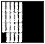
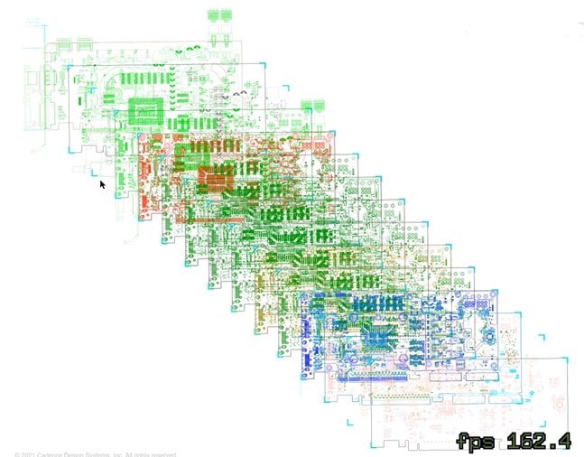
Anton went into some of the details of how Allegro used the Nvidia GPU boards to accelerate the rendering times, and they used a Scene Graph (SG) data structure. A PCB has many layers, each shown in different color below:

PCB Layers

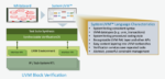
Accelerated rendering is done through a pipeline of several internal steps:

  • Allegro – incremental changes
  • Scene Mapper
  • Abstract Interface
  • NV Plugin – renderer
  • NV Plugin – QWindow + OpenGL context
  • Create and place rendering window

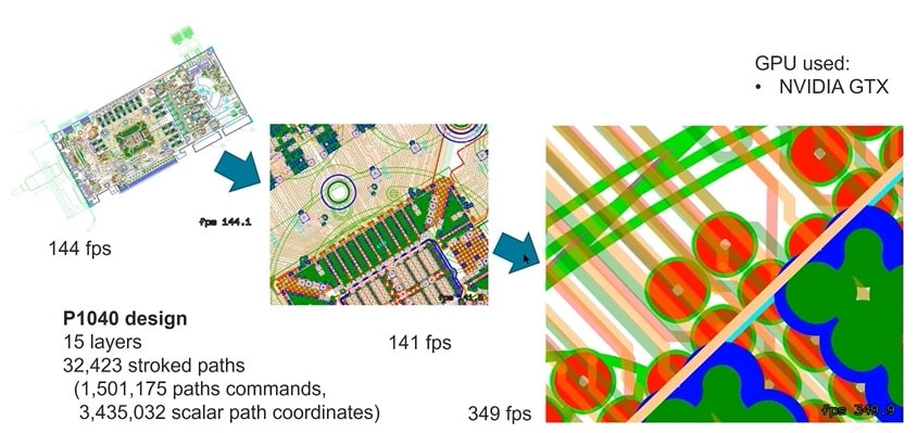
An example of how fast this GPU-based acceleration operates was shown with a 15 layer PCB design with 32,423 stroked paths, and Allegro had frame rates from 144 fps up to a whopping 349 fps, depending on the zoom level.

PCB NV Path Rendering

Even the text layers have acceleration for True Type Fonts with NV Path rendering. A technique called Frame Buffer Optimization (FBO) was also applied that understands the difference between a static and dynamic scene.

Results

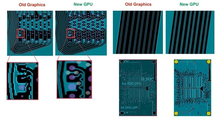
Patrick shared that GPU results often rendered instantly when using an Nvidia Quadro P2000 card, compared to a few seconds for the old graphic engine speeds. Quality of zooming into graphics was also much improved:

Quality improvements

With the old graphics approach there was a filter that identified objects less than 5-8 pixels, and simply didn’t show them at all. With the new GPU approach every single object is rendered, and there is no filtering, so there are fewer visual surprises to the designer when looking at their high-resolution monitors.

The Allegro tool ships with a demo board, and Patrick loaded that design and began to pan and zoom all around the board, with very little time spent waiting for all of the layers to render. The text was always crisp, and all objects were turned on.

Demo PCB

You can expect the GPU-based acceleration to be applied to future PCB challenges, like:

  • Shape engine
  • Design Rules Checker
  • Manufacturing output
  • Simulations

Allegro automatically detects if your workstation is using one of the popular Quadro series of GPUs (P, GP, GV, T, RTX) or the Tesla (P, V, T), so you just enjoy faster productivity.

Summary

Over the years in EDA I’ve watched CPU performance improve, cloud computing emerge, and GPU acceleration techniques added. They all have their place in making engineers and designers more productive by not having to wait so much time for results to become visible. Development engineers at Cadence in the Allegro group have done a good job of speeding up graphical rendering times for PCB designers by support GPU cards from NVIDIA.

Now the CAD department can buy NVIDIA GPU cards for their PCB designers and see immediate productivity improvements in Allegro operations. The bigger the project, the bigger the time benefits.

View the full 38 minute video online at Nvidia.

Related Blogs


WEBINAR: Balancing Performance and Power in adding AI Accelerators to System-on-Chip (SoC)

WEBINAR: Balancing Performance and Power in adding AI Accelerators to System-on-Chip (SoC)
by Daniel Nenni on 03-01-2022 at 6:00 am

Mirabilis Webinar AI SoC

Among the multiple technologies that are poised to deliver substantial value in the future, Artificial Intelligence (AI) tops the list.  An IEEE survey showed that AI will drive the majority of innovation across almost every industry sector in the next one to five years.

As a result, the AI revolution is motivating the need for an entirely new generation of AI systems-on-chip (SoCs).  Using AI in chip design can significantly boost productivity, enhance design performance and energy efficiency, and focus expertise on the most valuable aspects of chip design.

Watch Replay HERE


AI Accelerators
Big data has led data scientists to deploy neural networks to consume enormous amounts of data and train themselves through iterative optimization. The industry’s principal pillars for executing software – standardized Instruction Set Architectures (ISA) – however aren’t suited for this approach. AI accelerators have instead emerged to deliver the processing power and energy efficiency needed to enable our world of abundant-data computing.

There are currently two distinct AI accelerator spaces: the data center on one end and the edge on the other.

Hyperscale data centers require massively scalable compute architectures. The Wafer-Scale Engine (WSE) for example can deliver more compute, memory, and communication bandwidth, and support AI research at dramatically faster speeds and scalability compared with traditional architectures.

On the other hand, with regards to the edge, energy efficiency is key and real estate is limited, since the intelligence is distributed at the edge of the network rather than a more centralized location. AI accelerator IP is integrated into edge SoC devices which, no matter how small, deliver the near-instantaneous results needed.

Webinar Objective

Given this situation, three critical parameters for project success using AI accelerators, will be discussed in detail in the upcoming webinar on Thursday, March 10, 2022:

  • Estimating the power advantage of implementing an AI algorithm on an accelerator
  • Sizing the AI accelerator for existing and future AI requirements
  • The latency advantage between ARM, RISC, DSP and Accelerator in deploying AI tasks

An architect always thinks of the performance or power gain that can be obtained with a proposed design.  There are multiple variables, and many viable options available, with a myriad different configurations to choose from.  The webinar will focus on the execution of an AI algorithm in an ARM, RISCV, DSP-based system; and in an AI accelerator-based system.  The ensuing benefits of power, sizing and latency advantages will be highlighted.

Power Advantage of AI Algorithm on Accelerator using VisualSim
Mirabilis Design’s flagship product VisualSim has library blocks that have power incorporated into the logic of the block.  Adding the details of power does not slow down the simulation; it also provides a number of important statistics that can be used to further optimize the AI accelerator design.

VisualSim AI Accelerator Power Designer
VisualSim AI Accelerator Designer uses state-based power modeling methodology.  The user inputs two pieces of information – the power in each state (Active, Standby, Idle, Wait, etc.) and the power management algorithm.  As the traffic flows into the system and the tasks are executed, the instruction executes in the processor core and requests data from the cache and memory.  At the same time, the network is also triggered.

All these devices in the system move from one state to another.  VisualSim PowerTable keeps track of the power in each state, the transition between states, and the changes to a lower state based on the power management algorithm.

The power statistics can be exported to a text file, and to a timing diagram format.

Advantages of sizing the AI accelerator
AI accelerators are repetitive operations with large buffers.  These IPs occupy significant semiconductor space and thus augmenting the overall cost of the SoC, where the accelerator is just a small section.

The other reason for right-sizing of the accelerator is that, depending on the application, functions can be executed either in parallel or serial, or data size.  The buffers, cores and other resources of the IP must be sized differently.  Hence the right-sizing is important.

Workloads and Use Cases
The SoC architecture is tested for a variety of workloads and use-cases.  An AI accelerator receives a different sequence of matrix multiplication requests, based on the input data, sensor values, task to be performed, scheduling, queuing mechanism and flow control.

For example, the reference data values can be stored off-chip in the DRAM or can be stored in an SRAM adjacent to the AI block.  Similarly the math can be executed inline, i.e., without any buffering, or buffered and scheduled.

New VisualSim Insight Methodology and its Application
Insight technology connects the requirements to the entire product lifecycle by tracking the metrics generated at each level, against requirements.  The insight engines work throughout the process from planning, design, validation and testing.  In the case of the AI accelerator, the initial requirements can be memory bandwidth, cycles per AI, power per AI functions, etc.  Functional correctness and flow control correctness can be added later.  The goal of the Insight Engine is to carry metrics of system planning all the way to product delivery. There will be a reference to verify at each stage.

Building of AI Accelerators
AI accelerators can be built using a variety of configurations, whether single or multi-core.  A number of open-source concepts are available.  Companies such as Nvidia and Google have published their own accelerators.  The core IP from Tensilica provides AI acceleration as a primary feature.

Mirabilis Design and AI Accelerators
Mirabilis Design has experimented with performance and power analysis of Tensorflow ver 2.0 and 3.0. In addition, we are working on a model of the Tensilica AI accelerator model.

Workload Partitioning in Multi-Core Processors
The user constructs the models in two parts- hardware architecture and behavior flow which resembles a Task Graph.  Each element of a task can perform multiple functions- execute, trigger another task or move data from one location to another.  Each of these tasks get mapped to a different part of the hardware.  There are other aspects that will also affect the partition.  For example the coefficients can be stored locally, increased parallel processing of the matrix multiply, masking unused threads to reduce power etc.  The goal is to determine the number of operations per second.

Configuration Power and Performance Metrics
The power and performance do not follow the same pattern.  They can diverge for a number of reasons.  Memory accesses to the same bank group or writing to the same block address or using the same load/store unit can reduce die space and in some cases be faster, but the power consumed could be much higher.

Summary
Finally, we would like to say that this webinar apart from highlighting the above sections with regard to the AI accelerator, will also show how to arrive at the best configuration and detect any bottlenecks in the proposed design.

Watch Replay HERE

Also Read:

System-Level Modeling using your Web Browser

Architecture Exploration with Miribalis Design

CEO Interview: Deepak Shankar of Mirabilis Design


An Ah-Ha Moment for Testbench Assembly

An Ah-Ha Moment for Testbench Assembly
by Bernard Murphy on 02-28-2022 at 10:00 am

Forest Trees min

Sometimes we miss the forest for the trees, and I’m as guilty as anyone else. When we think testbenches, we rightly turn to UVM because that’s the agreed standard, and everyone has been investing their energy in learning UVM. UVM is fine, so why do we need to talk about anything different? That’s the forest and trees thing. We don’t need to change the way we define testbenches – the behavior and (largely) the top-level structure. But maybe there’s a better way to assemble that top level through a more structured assembly method than through hand-coding or ad-hoc scripting.

A parallel in design assembly

This sounds just like SoC design assembly. IPs are defined in RTL already, and you also want the top level in RTL because that’s the standard required by all design tools. But while top-level designs can be and should be defined in RTL, that is a cumbersome representation for assembly. Which is why so many design teams switch to spreadsheets and scripts to pull it together. Creation and updates are simpler through spreadsheets and scripts that handle the mechanical task of generating the final RTL.

UVM top levels present a similar problem for a different reason. The UVM methodology is very powerful and amply capable of representing a testbench top level. But it is a methodology defined by and for software engineers, full of object-oriented design and complex structures. All of which is foreign to the great majority of hardware verifiers who are not software experts. Worse still, UVM is sufficiently powerful that it does not constrain how components – VIPs, sequencers, scoreboards, etc. – define their interfaces. Which makes instantiating, configuring and hooking up these components a problem to be solved by the testbench integrator. Redundantly repeated between verification teams. This problem is well known. Verification teams typically spend weeks debugging testbenches before they can turn to debugging the design.

SoC verification requires that many testbenches be generated in support of the wide range of objectives defined in the test plan. Those objectives will be farmed out to multiple verification teams, often distributed across the globe. Most of whom are production verification engineers, not UVM experts. It is easy to see how effort you can’t afford to waste is wasted in support of an unstructured approach to testbench assembly.

Testbench assembly cries out for standardization

The Universal Verification Methodology is the foundation of any modern verification strategy. But few would deny that UVM, as a complex methodology designed around class-based design, is mystifying to the great majority of hardware verification engineers who are not experts in modern software programming concepts. A small team of UVM experts bridges the gap. They know how to construct the complex functions needed in SoC verification while also hiding that complexity behind functions or classes to make them more accessible to non-UVM-experts.

Complexity hiding is logical but is compromised by the diversity of sources for modern VIPs. Without a standard to align packaging methods, disconnects at the integration level are inevitable. In design assembly, the assembly problem has been significantly alleviated through the IP-XACT standard, defining a constrained and unified interface between components and the top-level assembly. Design and testbench structure have much in common, therefore IP-XACT should also be a good starting point to assemble testbench top levels.

Potential problems and solutions

One drawback is that there is no accepted standard today for packaging testbench components. Not that we don’t try. The in-house UVM team will develop components with interfaces to the in-house standard. Commercial VIP developers will each develop to their in-house standard. And there are legacy VIPs developed before any standard was considered. All well-intentioned, but this is a tower of Babel of interfaces. Some UVM teams go further, wrapping all VIPs in an interface following their protocol. A practical solution, though obviously, it would be better if we were all aiming at a standard and that redundant rework could be avoided. IP-XACT would be an excellent starting point, already well established for IP packaging.

A second potential problem is that IP-XACT has been defined for design, not testbenches. This is not nearly as big a problem as it might seem. Top levels should be mostly structural; IP-XACT already handles this very well through instantiations, ports, interfaces, connections, parametrization, and configurations. A couple of exceptions are class information exposed at the block level and SystemVerilog interfaces, both of which can be managed through vendor extensions. In the upcoming 2022 release, interfaces will be incorporated in the standard, leaving only class support to be handled in a later release, a goal which Arteris IP continues to push in the working group.

Interesting idea. What’s next?

Standardizing (and automating) testbench assembly is the only way to go to bring scalability to this task. UVM experts can work on building standard VIPs, leaving assembly (with much easier to understand scripting) to all those diverse teams in support of their needs.

Arteris IP has been developing a solution around this concept, with feedback from key customers. The result is Arteris Magillem UTG (UVM Testbench Generator). If you are intrigued and wonder if this approach could accelerate your SoC verification efforts, contact Arteris IP.

Also read:

Business Considerations in Traceability

Traceability and ISO 26262

Physically Aware SoC Assembly


Breker Verification Systems Unleashes the SystemUVM Initiative to Empower UVM Engineering

Breker Verification Systems Unleashes the SystemUVM Initiative to Empower UVM Engineering
by Daniel Nenni on 02-28-2022 at 6:00 am

SystemUVM Language Characteristics

The much anticipated (virtual) DVCON 2022 is happening this week and functional verification plus UVM is a very hot topic.  Functional Verification Engineers using UVM can enjoy a large number of benefits by synthesizing test content for their testbenches. Abstract, easily composable models, coverage-driven content, deep sequential state exploration, pre-execution randomization for test optimization and configurable reuse are just some examples of the advantages afforded by test suite synthesis.

However, a specification model is required and there are few alternatives that a UVM/SystemVerilog engineer can simply pick up and use.

Enter SystemUVM™, a UVM class library built on top of Accellera’s Portable Stimulus Standard that looks and feels like SystemVerilog with UVM, but enables the level of abstraction and composability required for this specification model with an almost negligible learning curve.

Breker Verification Systems Unleashes the SystemUVM Initiative to Empower UVM Engineering

Enhances Bug Hunting by Simplifying Specification Model Composition for Test Content Synthesis in Existing UVM Environments

SAN JOSE, CALIF. –– February 28, 2022 –– Breker Verification Systems used the opening of DVCon U.S. today to unveil SystemUVM™, a framework designed to simplify specification model composition for test content synthesis with a UVM/SystemVerilog syntactic and semantic approach familiar to universal verification methodology (UVM) engineers.

Developed in partnership with leading semiconductor companies, Breker’s SystemUVM’s UVM-style specification model drives test content synthesis, leveraging artificial intelligence (AI) planning algorithms for deep sequential bug hunting in existing UVM environments.

A coverage-driven approach simplifies test composition and employs up-front randomization for efficient simulation and accelerated emulation. It enhances test content reuse through configurable scenario libraries and portability for system-on-chip (SoC) integration verification and beyond.

For more information go to: www.brekersystems.com/SystemUVM

The Breker Approach
“UVM is an effective standard for block-level verification,” remarks David Kelf, Breker’s CEO. “As blocks and subsystems get larger and more complicated, composing test content for the UVM environment becomes more difficult and harder to scale. By leveraging synthesis for test content generation, a 5X improvement for larger components and multi-IP subsystems is common in composition time combined with significant coverage increases. SystemUVM makes this easily accessible for verification specialists with a minimal learning curve, dramatically changing the nature of functional verification.”

Breker’s SystemUVM layers UVM class libraries on to Accellera’s Portable Stimulus Standard (PSS) to provide the look and feel of SystemVerilog/UVM and its procedural use model. Models can be composed rapidly, efficiently reused and easily understood and maintained through UVM’s register access level (RAL), a library of common verification functions and abstract “path constraints.”

SystemUVM code offers an alternative to generic PSS while still being built on the industry standard, specifically targeting the needs of UVM engineers and recognizable to them, unleashing the power of PSS Test Content Synthesis tools, such as Breker’s TrekUVM™ and TrekSoC™ products.

SystemUVM-based Test Suite Synthesis allows the simplified generation of self-checking test content from a single abstract model complete with high-level path constraints for manageable code. Synthesis AI planning algorithms allow for specification state-space exploration, uncovering complex corner-cases that lead to potential complex bugs.

The coverage-driven nature of the process eliminates the need for coverage models and post-execution coverage analysis that results in test respins. With test randomization performed before execution, simulation is accelerated, and emulation can be used without an integrated testbench simulator, which increases its performance. The tests can also be reused in system verification via the Synthesizable VerificationOS layer without any change or disruption to the UVM testbench.

Availability and Pricing
SystemUVM is available today and is included in Breker’s Test Suite Synthesis product line. Pricing is available upon request. For more information, visit the Breker website or email info@brekersystems.com.

Breker at DVCon U.S.
DVCon’s tutorial “PSS In The Real World” opens this year’s virtual conference at 9 a.m. P.S.T., showcasing the power and flexibility of Accellera’s Portable Stimulus Standard by highlighting several real-world examples. Adnan Hamid, Breker’s executive president and CTO, is a speaker.

In-emulator UVM++ Randomized Testbenches for High Performance Functional Verification,” a Breker-sponsored workshop also on Monday at 11:30 a.m. P.S.T., attendees will learn proven, practical methods to verify complex blocks, SoCs and sub-systems with a high degree of quality.

The Meeting of the SoC Verification Hidden Dragons,” a panel organized by Breker and featuring Hamid will address the gap in semiconductor verification between block functional verification and system SoC validation. The panel will be held Wednesday, March 2, at 8:30 a.m. P.S.T.

About Breker Verification Systems
Breker Verification Systems is a leading provider of verification synthesis solutions that leverage SystemUVM, C++ and Portable Stimulus, a standard means to specify reusable verification intent. It is the first company to introduce graph-based verification and the synthesis of high-coverage test sets based on AI planning algorithms. Breker’s Test Suite Synthesis and TrekApp library allows the automated generation of high-coverage, powerful test cases for deployment into a variety of UVM, SoC and Post-Silicon verification environments. Case studies that feature Altera (now Intel), Analog Devices, Broadcom, IBM, Huawei and other companies leveraging Breker’s solutions are available on the Breker website. Breker is privately held and works with leading semiconductor companies worldwide.

Engage with Breker at:
Website:
 www.brekersystems.com
Twitter: @BrekerSystems
LinkedIn: https://www.linkedin.com/company/breker-verification-systems/
Facebook: https://www.facebook.com/BrekerSystems/

Also read:

Breker Attacks System Coherency Verification

Breker Tips a Hat to Formal Graphs in PSS Security Verification

Verification, RISC-V and Extensibility


Intel’s Investor Day – Nothing New

Intel’s Investor Day – Nothing New
by Doug O'Laughlin on 02-27-2022 at 6:00 am

https3A2F2Fbucketeer e05bbc84 baa3 437e 9518 adb32be77984.s3.amazonaws.com2Fpublic2Fimages2Fbe32664a cc3a 41e2 8898 d1a1ba57daf1 2400x1240

Intel’s big investor day was anything but big. The stock reacted poorly, down 5% on a day that was a widespread sell-off anyways.

I want to briefly summarize what matters for the stock. There was very little incremental news to the technology roadmap, and the financial outlook was underwhelming, to say the least.

The revenue guide was low single-digit growth, transitioning to mid-single-digit growth, to then double-digit growth in 2026.

They expect to improve gross margins when they get leadership products. They provided this simple bridge. David Zinsner (the new CFO) reiterated multiple times he thinks that this gross margin bridge was conservative.

The real meat of the financial outlook was given in a two-part long-term model. First, is the investment phase model, where they spend heavily to catch up to the industry and bootstrap their foundry business.

And then the longer-term model, when Intel presumably is back in the lead during their fateful 2024 crossover timeline. 2024 is when Pat Gelsinger believes they can take process leadership, and have better revenue growth and margins.

The thing is that the total vision was pretty underwhelming if you ask me. The reason why? Well, it’s consensus already.

It’s Consensus Already

One of the things that frustrated me is that I believe that the gross margin and revenue goals from the analyst day were within 50 bps of street consensus until 2025, and this is why the market found this model so particularly uncompelling. This is what we expected already, and stating it again felt pointless. This comment in particular was extremely off-putting as well.

“I want to double the earnings and double the multiple of this company”.

Historically commenting on the multiple is pretty icky if you ask me. Also if you compare it to the historical multiple it feels pretty unlikely. Will Intel really trade at 28x forward earnings?

Trading at 20x forward earnings would put it in a multiple class Intel hasn’t seen since pre-2008. Albeit growing double digits would also be something Intel hasn’t done since 2018 (~13% YoY revenue growth) and hasn’t done for a period of 3 consecutive years in a row since 2003-2005. There has to be a lot fundamentally different for Intel to deserve that doubling in multiple. We will talk about the doubling in earnings a bit.

Financial Model & Free Cash Flow Levers

The thing that also is a bit frustrating is looking at this company on an earnings basis when they guided for 3 years of flat to negative FCF. Here is my model backing out of their long-term guidance.

Notice doubling earnings from the 2022 level, not the 2021 level. For simplicity’s sake, I took the top end of their ranges. The conservatism that David and Pat stress I think is reflected by me assuming share count doesn’t grow.

So while it trades at “just 10x 2024 earnings” it will make no FCF in that year. There is so much implied in the model for the huge technical and financial turnaround in 2024. Everything in the model hinges on 2024 which is a few years away and implies a huge margin acceleration. From 0% FCF margin to 20% in 2 years, this seems unlikely.

The only thing that really made me believe this is possible is if they play the government incentives game really hard. Their initial capex guidance is based on 10% savings from net spend (their guide) to gross.

David Zinser also thinks that a 30% cost reduction number seems like the number they will get and would be “surprised” if Intel didn’t there.

So from my reading of this situation, Intel could hit the FCF number if they bag the entire savings from a 10% cost reduction to a 30% cost reduction, and then improve total EBIT margins by 800 bps. I think at least 1/3rd of the FCF bridge will be driven by playing around with the net and gross capex assumptions. Pretty heroic assumptions, which brings me to the entire crux of the investor day. We are waiting for 2024.

Waiting for Gadot (aka 2024)

The Intel turnaround is waiting for 2024. We kind of already knew that now we just have financial clarity until that fateful year. The financials were as bad as we expected, and for an Investor day, there was almost no surprise.

Another thing that I keep coming back to is that everyone expects that Intel’s turnaround will mean some drastic and amazing returns for the stock. To be clear if the turnaround happens with no hitches I think that the stock could easily do a 20%+ CAGR to 2026, but I also think that can be said of multiple companies in the semiconductor space at these current prices. I think the problem is that most investors are mentally comparing Intel to their notable competitor: AMD.

I want to be clear, this is not AMD. AMD went from almost no share to meaningful amounts of share and massively improved their economics in that time period. The torque of 10% to 40% share and 20% gross margins to 50% margins will not be repeated. The best case for Intel I think is something that is a 20%+ CAGR, or a rough tripling. That’s a great return! But I want to say this is the BEST CASE and is still contingent on a meaningful amount of execution risk and zero FCF for multiple years along the way. Investor day didn’t really give us much hope other than to wait until 2024.

We are still just waiting for 2024 to see the process leadership be regained.


Also, it looks like the crux of what I said about Tower tipping their hand of Intel becoming a holding company seems true.

The other thing I’ve said is that, “Hey, I’d like to do a Mobileye-like spin on our foundry business at some point as well.” I’m going to keep the structure, as opposed to integrating as much, I’m going to keep it more separate to enable that, which means I’m going to leverage a lot more of Tower and the expertise that it builds over time as part of it.

Ala the venerable Stratechery.

The screenshots from above are from a very simplistic model that I used to replicate the investor day goals. It is behind the paywall for paying subscribers only. Feel free to mess with the assumptions yourself. The FCF part of the model is disconnected from earnings, mostly because of how meaningful the D&A cost ramp will be for the next few years.

Subscribe

Also Read:

Semiconductor Earnings Roundup

Tower Semi Buyout Tips Intel’s Hand

The Rising Tide of Semiconductor Cost

TSMC Earnings – The Handoff from Mobile to HPC


Podcast EP64: The real story behind Fairchild Semiconductor

Podcast EP64: The real story behind Fairchild Semiconductor
by Daniel Nenni on 02-25-2022 at 10:00 am

Dan is joined by John East, the former CEO of Actel. In the sixth episode of Semiconductor Insiders John explained the beginnings of Fairchild Semiconductor and the significance of the Traitorous Eight.

In this follow-up discussion, John recounts the rise and fall of Fairchild Semiconductor. This is a turbulent and significant chapter in semiconductor history. John’s eye-witness account is revealing, entertaining and thought-provoking. These are some of the stories in John’s new book. The details of that are discussed as well. A key lesson conveyed in the discussion is the difference between knowing how to make semiconductors vs. knowing what semiconductors to make.

The views, thoughts, and opinions expressed in these podcasts belong solely to the speaker, and not to the speaker’s employer, organization, committee or any other group or individual.


CEO Interview: Tamas Olaszi of Jade Design Automation

CEO Interview: Tamas Olaszi of Jade Design Automation
by Daniel Nenni on 02-25-2022 at 6:00 am

Tamas Olaszi
rpt

Why does the industry need another register management tool? This is a question that Tamas Olaszi, the founder of Jade Design Automation hears from time to time since Jade-DA brought Register Manager, their EDA tool, to market. So why?

There is a genuine answer to this question but first let me use this interview to give some helpful information to the Semiwiki audience. Some people will come here while looking for a new register management solution for a startup or replace an existing solution that has some issues. I would like to give them an overview of this space so they can make an informed decision. What commercial register management tools are out there? How to manage the HW/SW interface? How to generate Verilog from CSRs? Is there an open source SystemRDL tool? Can we use IP-XACT for capturing our register descriptions?

Ok, so who are the commercial tool vendors in this space?

At the time of this interview, in alphabetical order they are Agnisys, Jade Design Automation, Magillem (acquired by Arteris now) and Semifore. However, the history here is quite interesting. Commercial tools for register management started to appear around 2006-2008. Jade-DA was not around at that time but the other three started roughly at the same time. There was a fourth player though, called Duolog Technologies and I was working there as a Hardware Design Engineer when Duolog launched its Bitwise product. I transitioned into an FAE role supporting Duolog’s register management tool and lived and worked in India, France, US and Ireland as well in the subsequent years. I had the chance to see the adoption of these tools by various semiconductor companies around the globe and gather first hand customer feedback. Duolog was doing quite well with its EDA tools and the company was acquired by Arm in 2014 which stirred up things a little bit.

At Arm, I first was responsible for an internal tooling team and we were developing and customizing register management and SoC assembly tools for Arm’s specific needs. I then moved on to manage an open source embedded software team responsible for writing the SW for the IoT test chips of Arm. This was also very educational to me as I now have been involved in the last piece of the HW/SW interface jigsaw puzzle – I have experienced the full workflow from the first time when the System Architect drafts up the top level memory map to the last bit when the SW engineers checks in the last driver code for the Board Support Package to bring up the chip. I thought my tooling days were behind me at this stage but then on a sunny Tuesday morning Arm announced that it would discontinue the Duolog EDA product line.

This was an understandable move from an IP company that acquired an EDA company – they repurposed the tools they needed to do IP configuration and discontinued the ones that were not related to the core business. This proved to be a seminal moment for me and this led eventually to the founding of Jade Design Automation.

You mentioned that you were leading an internal tooling team. Shouldn’t internal tools be right choice for register management?

They can be. Really, the main advantages of the internal solution is that it is tailored to the company’s needs and that the support is that nice person sitting two seats away from you. This kind of flexibility has a very real value and it is a cliche in our industry that our biggest competitor is the internal solution. Many great people came up with many great solutions at different companies.

The risk here is maintenance. Those aforementioned great people may get promoted, would like to take their career in a different direction or change jobs. There is also a cost which is invisible because it is not monetary but opportunity cost. Usually the person maintaining the internal solution is a very capable HW design or verification engineer who could work on the core business of the company.

Then there are other free alternatives like various open source solutions. What do you think about those?

Again, those could be a viable alternative as well. There are many of them and I am going to list the few here that I know of in order to help people evaluate their options. At various stages I came across airhdl, pyrift, a register tool in the Open Titan project and systemrdl-compiler. Out of these, SystemRDL Compiler is the project I followed more closely and I greatly admire the work of the guy who is behind the project.

What I have heard from talking to people is that these open source projects tend to become the basis of an internal tool. They are great for jump starting the deployment of a register management solution but they usually need to be tailored to the company’s needs so they kind of get forked internally and built upon.

So with these, how would a company select a register management solution?

I suppose the factors they need to take into account are the following:

  • Data model – should it be a standard like IP-XACT or SystemRDL or proprietary that offers more flexibility
  • Features – what kind of generators they need, how big their designs, what are their performance requirements, do they need a GUI, etc.
  • Flexibility – it is very likely that every solution out there will need some level of customization so it is important to know how easy it is to custom fit the solution
  • Support – I suppose the turnaround time matters here the most, whether getting a fix to a problem takes two days or two months
  • Cost – which is self explanatory

The commercial vendors all made their decisions regarding the data model, the tool architecture and the business model. The open source solutions can also be evaluated along these criteria and of course the internal solution leaves all these open.

Can we get an answer now to the original question? Why does the industry need another register management tool?

At that moment when it was announced that Arm would discontinue the Duolog EDA line, I felt that this could be a great opportunity. The team there built up a lot of experience in the domain of register management both with a small EDA company supporting customers worldwide and as part of an internal tooling team of a major semiconductor company. There was the chance to build something new that would incorporate all these experiences into a tool built on a modern data model with modern technologies.

The fact that there is still a plethora of different solutions out there, commercial, internal and open source alike shows that this problem is still not convincingly solved. Most solutions stop at about 80% where it is “good enough” for that particular company or individual – but not necessarily for everyone else. In my vision, it is possible to have the holy grail of data models that cover almost all of the required constructs across the industry and leave only the last mile to a flexible customization framework. With that, we could reach a de-facto standard for register management which would also enable seamless transfer of register data within the ecosystem.

With this interview, I didn’t want to pretend that we exist in a vacuum. Our potential customers have a variety of options to choose from. There are all these factors of data model, feature set, flexibility, support and cost that they need to take into account and each company puts different weight on them. I am happy to lay all the cards on the table because I am quite confident that Jade Design Automation’s Register Manager can compete head-on with any of the alternatives.

https://jade-da.com/

Tamas Olaszi, the founder of Jade Design Automation, started his career as a HW design and verification engineer at an Irish design service company. Along with the company, he pivoted into the world of EDA working as a Field Application Engineer while living and working in India, France, Ireland and the US for several years. Along these years he worked closely with companies like Texas Instruments, Qualcomm, Western Digital and Nokia among others. After the company’s acquisition, he worked at Arm for five years where he was responsible for building up and managing an open source embedded SW team with a remit of building a secure SW foundation for the IoT test chips of Arm. Since founding Jade Design Automation in 2019 he is working towards a vision of a register management tool that outperforms all of the alternatives in all the relevant metrics.

Also read:

CEO Interview: John Mortensen of Comcores

CEO Interviews: Kurt Busch, CEO of Syntiant

CEO Interview: Mo Faisal of Movellus


Integrated 2D NoC vs a Soft Implemented 2D NoC

Integrated 2D NoC vs a Soft Implemented 2D NoC
by Kalar Rajendiran on 02-24-2022 at 10:00 am

Routing of cnv2d design using Speedster7t 2D NoC

We are living in the age of big data and the future is going to be even more data centric. Today’s major market drivers all have one thing in common: efficient management of data. Whether it is 5G, hyperscale computing, artificial intelligence, autonomous vehicles, or IoT, there is data creation, processing, transmission, and storage all around us. All of these aspects of data management need to happen very fast.  Data center operators cannot afford to tolerate data traffic jams anywhere in the data path. They need to process incoming data efficiently and move the data to its destination rapidly. The underlying system hardware architecture design is a critical factor in allowing rapid data transfer.  Therefore, the selecting of the right processing architecture will have a major impact on performance.

SemiWiki has covered the Achronix Speedster7t FPGA devices and their various features in several posts because of their innovative 2D NoC features.  For rapidly moving data throughout a chip, there is little contention that a Network-on-Chip (NoC) is an excellent approach. A NoC architecture is better at moving data than a conventional bus architecture and a crossbar architecture. But should you implement your own 2D NoC on an FPGA fabric or leverage a pre-built 2D NoC? Is one 2D NoC implementation better than another? This is the question that Achronix answers in a recently published whitepaper titled “The Achronix Integrated 2D NoC Enables High-Bandwidth Designs.” Of course, the comparison study is between Achronix’s own 2D NoC and a soft implemented 2D NoC on their Speedster7t family of FPGAs. This post is a synthesis of what I gathered from the whitepaper.

The Contender 2D-NoC

The soft 2D NoC chosen for the comparison project is from Milan Polytechnic (https://github.com/agalimberti/NoCRouter, 2017) based on peer reviews and ease of portability to an FPGA fabric. It implements a wormhole lookahead predictive switching in a unidirectional mesh.

Benchmark Design

To quantify the differences between the Speedster7t 2D NoC and the soft implementation using FPGA fabric resources, a two dimensional convolution (Conv2d) design was created. This design performs AlexNet 2D convolution on an input image and contains 19 instances the Conv2d design.

The Metrics Used for Comparison

The metrics that are picked for comparison of any two solutions should be relevant and important to the solutions’ users. In the context of what is being compared, the following metrics were chosen:

  • How many resources are needed for each of the two solutions?
  • What is the performance of the design using each solution?
  • How long does it take to design and compile the design?

Results from Achronix’s 2D NoC Comparison Study

Performance

The use of the integrated 2D NoC produces an elegant, repeatable structure to place and route the design that results in regular routing with less congestion. Refer to Figure below. Using the Achronix’s integrated 2D NoC achieves a maximum frequency of 565MHz for the Conv2d design.

Routing of the Conv2 Design Using the Achronix Integrated 2D NoC

Compare the above with the complex, irregular and congested routing when using the soft implemented 2D NoC. Refer to Figure below. Timing is also compromised as deep LUT logic is needed to select the appropriate paths in the soft implemented 2D NoC.

Routing of the Conv2d Design Using the Soft Implemented 2D NoC

Design and Compile Time

The full-featured implementation of the Achronix integrated 2D NoC eliminates a large amount of design work for the users. For example, built-in features such as clock-domain crossing logic, transaction flow control, and decoding of addresses. This allows designers to concentrate just on the value added user logic connecting to the 2D NoC. Along with reduced design time, a design that utilizes the Achronix integrated 2D NoC uses fewer resources than one that uses a soft implemented 2D NoC. The result is less logic to place and route, and results in faster compile time through the tools.

Summary

The Speedster7t architecture significantly improves design productivity while making the Achronix FPGAs very effective for high-bandwidth applications. The designs benefit from reduced logic utilization, reduced memory requirements and increased performance. You can download the whitepaper here. Refer to the table below for the results from the comparative study.

Conv2d Design and Comparison of the 2D NoCs

Also read:

2D NoC Based FPGAs Valuable for SmartNIC Implementation

Five Reasons Why a High Performance Reconfigurable SmartNIC Demands a 2D NoC

Take the Achronix Speedster7t FPGA for a Test Drive in the Lab


Scalable Verification Solutions at Siemens EDA

Scalable Verification Solutions at Siemens EDA
by Daniel Nenni on 02-24-2022 at 6:00 am

Andy Meier 2

Lauro Rizzatti recently interviewed Andy Meier, product manager in the Scalable Verification Solutions Division at Siemens EDA. Andy is a product manager in the Scalable Verification Solutions Division at Siemens EDA. Andy has held positions in the electronics and high-tech fields during his 20-year career including: Sr. Product Marketing manager at Siemens EDA, Product Marketing manager at Mentor Graphics, Solution Product manager at Hitachi Data Systems, Director of Application engineering at Carbon Design Systems, and Sr. Verification Engineer at SiCortex. He holds a Bachelor of Science degree in Engineering and Computer Engineering from Worcester Polytechnic Institute in Worcester, Mass.

Thank you for meeting with me, Andy. It is a pleasure to talk with you. One of the major challenges SoC verification and validation teams has is ensuring correct system operation with real workloads. What is at the core of this challenge?

The core of this challenge comes down to the fact that hardware and software teams have different perspectives and different debug needs when tasked with ensuring correct system operation. Often hardware and RTL design teams rely on waveforms to debug while software developers need a full-functioning software debugger. The problem is when there is an issue that they both need to be involved in, such as debug, each set of users is speaking a different debug language. They need a way to speak a common debug language and correlate between both the hardware teams and the software teams.

How is it possible for them to so call, speak a common language?

In our Codelink product, we have a correlation engine that allows our customers to do just that. It is one of the greatest strengths of Codelink. As I said the SW team is looking for a full functioning SW debugger. Being able to single step the SW execution while looking at a source code view, CPU registers and memory views of what is happening in the SoC is invaluable. To then be able to correlate that to exactly what is happening at the RTL level by looking at the waves is extremely powerful. This is what truly enables the HW/SW co-verification use case.

Can you share a real-world customer example of the HW/SW co-verification use case?

Recently, a customer came to us with a unique challenge. This customer had a six-stage boot process that jumped from CPU to CPU through the ‘power on’ sequence where the CPUs came from different vendors. Ultimately, they were tasked with integrating the IP as well as validating the multi-stage boot process of their SoC. The customers existing verification and validation methodologies didn’t have a unified way to debug this scenario. They would look at waveforms from one simulation or emulation run at a specific stage, and then use different tool sets from different CPU vendors to debug the following stage. There was no common unified debug. To make matters more challenging, the team involved in this verification and validation effort was the SoC integration team. This team didn’t have domain expertise of the hardware design, and they didn’t have the software expertise on what individual blocks were responsible for what. Still, they were tasked with validating and making sure that the SoC booted properly. They were interested in using a new solution to address their needs.

Using standard features from Codelink, like the source code view, the register view, and the correlation engine  as well as RTL Waves from an emulation run, the customer created and adopted a new methodology focused on unifying their debug. Using this new methodology, they were able to look at the multi-core capabilities of their SoC and debug the software execution as it jumped through the various stages to ensure things were operating as expected.

That’s quite interesting. Beyond what you just described, what are some current industry trends that present other challenges?

In terms of trends, we see the use cases expanding beyond just traditional SW debug and HW/SW co-validation. Customers have expanding SoC requirements, and these requirements are driving new opportunities for expansion of SW-enabled verification.

For example, customers are trying to understand how their software is performing. They are trying to understand the behavior of different event handlers execution, and if those event handlers are executing within the budgeted amount of time. To address this additional use case in an emulation environment, we have added into our Codelink tool software performance profiling. This allows customers to identify where the time is being spent, and the functions that are called most frequently. This is key for customers that are working on hardware and software partitioning or customers trying to tune their SoC performance. One can imagine a case where an event handler is supposed to execute within a certain amount of time, but for one reason or another, it doesn’t. The customer can now isolate where the time is being spent from a software perspective, and then tune the performance.

We’ve also recently seen from both simulation and emulation customers, where providing SW code coverage helped aid in the SW verification and validation. An example where this was used, was when the customer’s SW-enabled verification methodology had randomly generated SW in it. The randomly generated SW acted like test vectors for their SoC. Due to its random nature, the customer needed to know exactly what SW test scenarios had been covered and executed. We’ve added SW code coverage to Codelink to address this need. All that was needed from the customer was the software executable and debug symbols, which they already needed to execute the workload. The validation team can now look at the SW Code coverage report and see what statements, functions, conditions, or branches were covered during the execution.

What other industry trends are you seeing?

With different SoC market verticals, such as automotive, IoT, 5G, Enterprise Data Centers, etc., we have seen a need to increase our collaboration with our CPU IP partners. Over time, we’ve built strong partnerships in collaboration with different IP suppliers to provide Codelink debug capabilities for those CPU IPs. Recently we have seen a significant increase in requests for RISC-V CPU support from the RISC-V community. In collaboration with SiFive, we have been able to add Codelink support for several SiFive CPUs. This is just one example. By being CPU IP vendor agnostic, it allows us to work with all the IP vendors to meet the customers needs.

There is some interesting work going on in this space, Andy. Thank you again for your time. Maybe we can catch up in a year and look at your continued progress.

Also read:

Power Analysis in Advanced SoCs. A Siemens EDA Perspective

Faster Time to RTL Simulation Using Incremental Build Flows

SIP Modules Solve Numerous Scaling Problems – But Introduce New Issues


Working with the Unified Power Format

Working with the Unified Power Format
by Daniel Payne on 02-23-2022 at 10:00 am

UPF design flow min

The Accellera organization created the concept of a Unified Power Format (UPF) back in 2006, and by 2007 they shared version 1.0 so that chip designers would have a standard way to communicate the power intentions of IP blocks and full chips. By 2009 the IEEE received the Accellera donation on UPF , reviewed multiple drafts and published IEEE Std 1801-2009, also known as UPF 2.0. In 2013 the IEEE updated it to 1801-2013, or UPF 2.1. Updates to UPF continued into 2015 and 2018 as well.

Why do we even need UPF? 

RTL languages like VHDL and SystemVerilog don’t include the notion of power intent, just logic functionality, so something needed to be added for power intent. Here’s an EDA tool flow showing where power intent files are used during design, verification and even implementation:

Source: IEEE

What’s Inside a UPF File?

Power intent is defined using an extension of the Tool Command Language (Tcl) and has the following components:

  • Power Domains
  • Power Supply Network
  • Power State Table
  • Isolation Strategies
  • Retention Strategies
  • Level Shifter Strategies
  • Repeater Strategies

Who Creates UPF Files?

Your IP vendors supply RTL code, and constraint UPF file, then your design team adds a  configuration UPF file for the specific context. Implementation-specific UPF files are also added along the way, so the EDA tool flow becomes:

UPF files and tool flow

How about using Hierarchy?

UPF supports both flat and hierarchical descriptions, and in general it’s recommended to align power domains with your logic hierarchy to keep life simple. If you choose to implement your design from the bottom-up, then ports need to be added in your UPF descriptions.

In a traditional bottom-up methodology an engineer would read all of the UPF files, then start manually editing each UPF file to ready them for merging into a top file. The UPF top-level file would be manually created, with care made to verify that proper syntax was typed. The power rules would also be verified before and after promotion.

Here’s a diagram showing a simple chip design example with four instances, named A, B, C, D; and at the top-level you can describe this with either hierarchy (left side), or as a flat design (right side):

UPF hierarchy or flat

With the hierarchy example on the left, we have five UPF files, while in the flat example on the right only one UPF file. Switching between using UPF hierarchy or flat is called promotion or demotion, and as you can imagine involves some detailed Tcl editing. Sure, you could manually do these operations and hope that you got all of the edits correct, or you could use an EDA tool designed for this purpose.

Going from a single, flat UPF file to a hierarchical collection of UPF files is called demotion, and once again, there is manual editing required. If any RTL code is modified during this process, then that adds more UPF file editing.

Thanks to EDA vendor Defacto Technologies we now have such an EDA tool to manage jointly UPF and RTL pre-synthesis through SoC Compiler. During the front-end SoC build process a design team has many files to manage, and SoC Compiler enables an engineer to quickly work with RTL, IP-XACT, UPF and SDC files.

With SoC Compiler an engineer can easily manage power-intent hierarchy, out of the box, with two simple APIs: promote_power_intent, demote_power_intent. Typical applications where UPF promotion and demotion are used in a project include:

  • When exporting an IP block from an SoC for reuse
  • Integrating multiple IPs into an SoC
  • Using hierarchical synthesis

Summary

They say that necessity is the mother of invention, and the development team at Defacto has taken a look at how the UPF standard came about, and noted that processes like promotion and demotion to work with hierarchy has required far too many manual, error-prone editing steps. Their UPF automation embodied in the SoC Compiler tool provides much-needed relief to SoC teams by quickly using UPF promotion or demotion.

Webinar

There’s a March 10th webinar from 10AM to 11AM PST all about SoC Compiler from the team at Defacto Technologies, so sign up here.

Related Blogs