In 1982, Richard Feynman, a theoretical physicist and Nobel Prize winner, proposed the initial quantum computer; Feynman’s quantum computer would have the capacity to facilitate traditional algorithms and quantum circuits with the goal of simulating quantum behavior as it would have occurred in nature. The systems Feynman wanted to simulate could not be modeled by even a massively parallel classical computer. To use Feynman’s words, “Nature isn’t classical, dammit, and if you want to make a simulation of nature, you’d better make it quantum mechanical, and by golly it’s a wonderful problem, because it doesn’t look so easy.”
Today, companies like Google, Amazon, Microsoft, IBM, and D-Wave are working to bring Feynman’s ambitious theories to life by designing quantum hardware processing units to address some of the world’s most complicated problems—problems it would take a traditional computer months or even years to solve (if ever). They’re tackling cryptography, blockchain, chemistry, biology, financial modeling, and beyond.
The scalability of their solutions relies on a growing number of qubits. Qubits are the building blocks of quantum processing; they’re similar to bits, the building blocks of traditional processing units. IBM’s roadmap for scaling quantum technology shows the 27-qubit IBM Q System One release in 2019, and less than 5 years later, they expect to release the next family of IBM Quantum systems at 1,121 qubits.
Achieving a sufficient level of qubit quality is the main challenge in making large-scale quantum computers possible. Today, error correction is a critical operation in quantum systems, and it preoccupies the vast majority of qubits in each quantum processor. Improving fault tolerance in quantum computing requires error correction that’s faster than error occurrence. Beyond error correction, there are plenty of challenges on the road to designing a truly fault-tolerant quantum computer with exact, mathematically accurate results. Qubit fidelity, qubit connectivity, granularity of phase, probability of amplitude, and circuit depth are all important considerations in this pursuit.
While quantum computing poses a major technological leap forward, there are similarities between quantum designs and traditional IC designs. Those similarities allow the electronic design automation (EDA) industry to build on existing knowledge and experience from IC workflows to tackle quantum processing unit design.
Logic Synthesis in Quantum and RFIC Designs
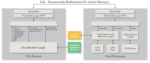
In quantum designs on superconductive silicon, the basic building block is the Josephson Junction. In radio-frequency integrated circuit (RFIC) chips, that role is played by transistors. In both situations, these fundamental building blocks are used to build gates that ultimately form qubits in quantum and bits in RFIC.
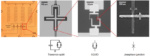
Image source: “An Introduction to the Transmon Qubit for Electromagnetic Engineers”, T. E. Roth, R. Ma, W. C. Chew, 2021, arXiv:2106.11352 [quant-ph]
Caption: From the Josephson junction to the quantum processor
In RFICs, the state of a bit can be read with certainty—it’s either 0 or 1. Determining the state of a qubit is much more complicated. Yet, it’s a critical step for accurate calculations. Due to the peculiar laws of quantum mechanics, qubits can exist in more than one state at the same time—a phenomenon called superposition. Superposition allows a qubit to assume a value of 0, 1, or a linear combination of 0 and 1. It’s instrumental to the operations of a quantum computer because it provides exponential speedups in memory and processing. The quantum state is represented inside the quantum hardware, but when qubits are measured, the quantum computer reports out a 0 or a 1 for each.
Entanglement is another key quantum mechanical property that describes how the state of one qubit can depend on the state of another. In other words, observing one qubit can reveal the state of its unobserved pair. Unfortunately, observation (i.e., measurement) of the state of a qubit comes at a cost. When measuring, the quantum system is no longer isolated, and its coherence—a definite phase relation between different states—collapses. This phenomenon, quantum decoherence, is roughly described as information loss. The decoherence mechanism is heavily influenced by self and mutual inductance among qubits, which must be modeled with very high accuracy to avoid chip malfunctions.
Quantum processors are frequently implemented using superconductive silicon because it’s lower in cost and easy to scale. Further, it offers longer coherence times compared to other quantum hardware designs. In this implementation, integrated circuits (ICs) are designed using traditional silicon processes and cooled down to temperatures very close to zero Kelvin. Traditional electromagnetic solvers struggle with the complexity and size of quantum systems, so simulation providers need to step up their capacity to meet the moment.
Image credits: IBM
Caption: An IBM quantum computer
Modeling Inductance in Quantum and RFIC Designs
It’s worth noting that superconductors are not new, exotic materials. Common metals like niobium or aluminum are found in superconducting applications. Once these metals are cooled down to a few millikelvin, using a dilution refrigerator, a portion of their electrons do not flow as they normally would. Instead, they form cooper-pairs. This superconductive current flow results in new electromagnetic effects that need to be accurately modeled. For example, inductance is no longer simply the sum of self and mutual inductance. It includes an additional term, called kinetic inductance:
This summation is not as straightforward as it looks. Kinetic inductance has drastically different properties than self and mutual inductance, which are frequency independent and temperature dependent. In a similar fashion, the minimal resistance in a superconductor has different properties than the ohmic resistance of conductors (i.e., proportional to the square of frequency). Electromagnetic modeling tools must account for these physical phenomena both accurately and efficiently.
Scale also poses challenges for electromagnetic solvers. Josephson Junctions, the basic building block of the physical qubit, combine with superconductive loops to form qubit circuits. The metal paths form junctions and loops with dimensions of just a few nanometers. While qubits only need a tiny piece of layout area, they must be combined with much larger circuits for various operations (e.g., control, coupling, measurement). The ideal electromagnetic modeling tool for superconductive hardware design will need to maintain both accuracy and efficiency for layouts ranging from several millimeters down to a few nanometers to be beneficial in all stages of superconductive quantum hardware design.
Image source: “Tunable Topological Beam Splitter in Superconducting Circuit Lattice”, L. Qi, et.al., Quantum Rep. 2021, 3(1), 1-12
Caption: An indicative quantum circuit
Looking Forward (or backward – It’s hard to tell with Quantum)
Designers in the quantum computing space need highly accurate electromagnetic models for prototyping and innovation. Simulation providers need to rise to the challenge of scaling to accommodate large, complex designs that push the boundaries of electromagnetic solvers with more and more qubits.
Ansys, the leader in multiphysics simulation, recently launched a new high-capacity, high-speed electromagnetic solver for superconductive silicon. The new solver, RaptorQu, is designed to interface seamlessly with existing silicon design flows and processes. Thus far, our partners are particularly pleased with their ability to accurately predict the performance of their quantum computing circuits.
Caption: Correlation of RaptorQu with HFSS on inductance (left) and resistance (right) for a superconductive circuit
Interested? For updates, keep an eye on our blog.
Dr. Kostas Nikellis, R&D Director at Ansys, Inc., is responsible for the evolution of the electromagnetic modeling engine for high speed and RF SoC silicon designs. He has a broad background in electromagnetic modeling, RF and high-speed silicon design, with several patents and publications in these areas. He joined Helic, Inc. in 2002, and served as R&D Director from 2016 to 2019, when the company was acquired by Ansys, Inc. Dr. Nikellis received his diploma and PhD in Electrical and Computer Engineering in 2000 and 2006 respectively, both from the National Technical University of Athens and his M.B.A. from University of Piraeus in 2014.
Kelly Damalou is Product Manager for the Ansys on-chip electromagnetic simulation portfolio. For the past 20 years she has worked closely with leading semiconductor companies, helping them address their electromagnetic challenges. She joined Ansys in 2019 through the acquisition of Helic, where, since 2004 she held several positions both in Product Development and Field Operations. Kelly holds a diploma in Electrical Engineering from the University of Patras, Greece, and an MBA from the University of Piraeus, Greece.
Also Read:
The Lines Are Blurring Between System and Silicon. You’re Not Ready.
Multiphysics, Multivariate Analysis: An Imperative for Today’s 3D-IC Designs
A Different Perspective: Ansys’ View on the Central Issues Driving EDA Today


