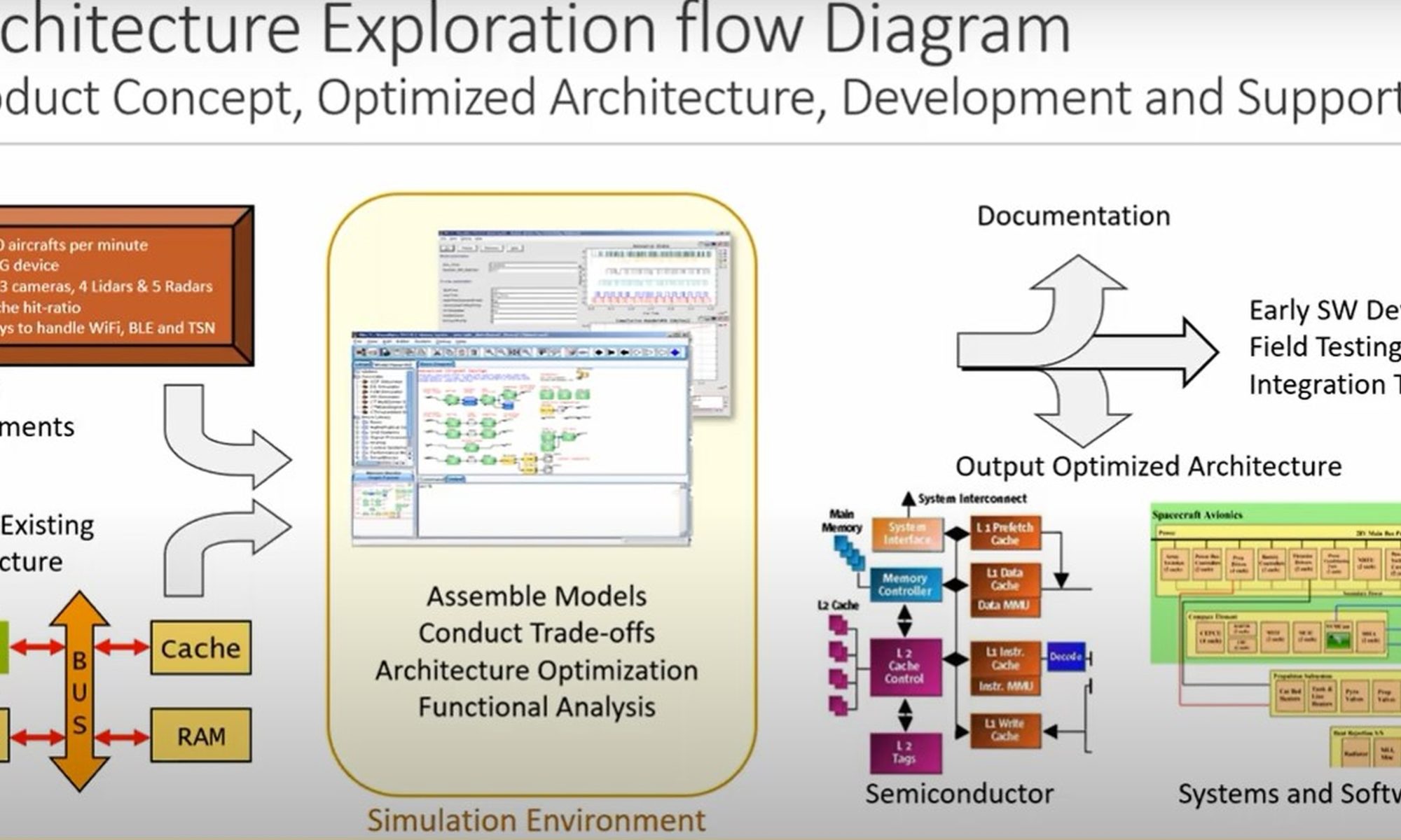

Architectural exploration is a vast area of engineering design. It starts with the planning phase where the designer will have the list of requirements from the customer and the rough architecture most likely on a paper. Next is to assemble the model and conduct variety of trade-offs for optimization and functional studies to meet the specified requirements. It may technical or business requirement or the cost. Architecture expiration code now goes to three states:
- a) Generates documentation.
- b) Development of the specification either by an internal team or an external partner which can be at the semiconductor level embedded systems or software level.
- c) Provides a platform for early software development, field testing, integration testing and a variety of other requirements that come along the product development flow.

Fig 1: Architecture exploration flow diagram from Mirabilis Design
Figure 1 displays an architectural exploration flow diagram. A typical system is going to consist of three parts: a) communication b) computation and c) scheduling.
Communication typically includes the topology, fabric, busts, and knobs. It may be at a board, a network or a semiconductor. For instance, the first part of the image in figure 2 shows different communication templates like the ring, shared bus, and a complete embedded system distributed network. The second part displays a whole variety of devices that would exist on the system like Graphics Processing Unit (GPU), Field Programmable Gate Array (FPGA), Central Processing Unit (CPU), Dynamic Random Access Memory (DRAM) etc. Finally, the last part exhibits different types of scheduling/arbitration flow control.

Fig 2: Components of a System Architecture.
There are multiple architectures available. Three things must be taken into consideration before choosing of an architecture.
- a) The traffic
- b) The workflow and
- c) The specified requirement the designer need to attain like lower latency, higher throughput, lower energy, lower power or the overall cost.
Based on these criteria’s one can evaluate which architecture is more suitable for a particular application. A particular product for instance a SSD system, may have different architecture requirements. Depending on whether it is going into the mobile or the data center or the desktop the form factor, cost, performance, and throughput can be completely different for the same product.
Architecture exploration can be used across every application space where electronics is used. For instance, it can be used for a card network, a rocket, or a semiconductor component like a power processor.
Requirements for architectural exploration
Architecture exploration starts from an early conceptual stage and can goes down all the way through the product development flow. This can be explained with the help of a diagram.

Fig 3: Architectural Exploration Methodology using System Modeling software such as VisualSim Architect
Due to early analysis of requirements, the designer need not be worried about components. At this stage the key concern is how to translate the requirements into an engineering market. Next step is to focus on the performance and power optimization, to reckon the trade-offs, for instance the failure and functional analysis, security, and a variety of other attributes. The designer exactly can detect what is going to be the minimum latency or the highest throughput that can be achieved. After this point, hardware and software partitioning is done in order to split the data across multiple subsystems or across multiple IPs and on a chip or across multiple boxes. After dividing the portions of software and hardware, select different components, schedule the arc tosses and assemble a complete system. If there is a c code or an emulator that has some technology at this point, then that can be integrated to create a single environment.
Architecture Exploration phases
Architecture exploration can be divided into four parts.
- Model based System Design
- Electronic System-Level Design
- Virtual Prototyping
- Hybrid Prototyping

Fig 4: Architecture Exploration Phases
Model Based System Design can be applied to vehicle networking, mission level, networked systems, and data centers. In vehicle networking, it connects the internals like the gateways, the network etc. that are within the car and the externals systems like the Wi-Fi, satellite communication etc., at the same time into one model. Similarly, at mission level, you must build a network that connects multiple aircrafts, satellites, and ground stations together. In case of networked systems data centers, one need to connect the IOT systems or semiconductor vendors, chips together into a single model. So, the goal is to provide a solution, not just about what’s inside of the chip or inside of the box but also what is the performance when one communicates with the datacenter. This can be done at early stage of design process.
For electronics system level design, one can design the semiconductor, the hardware, and the software like designing of the artificial intelligence score or to put an entire chip together or to integrate multiple systems and boards together. So, looking at end to end of every aspect is important to get a good quality product.
Virtual prototyping is using of something that already exists in the system and the designer want to use it onto a new design. It may be a software or modify an old software to work on a new design. Or the designer has decided on a design, and he want to check whether the diagnostics is sufficient. Or even if he wants a platform to run the software and check the functionality. The designer can evaluate performance improvement or power saving from software update. For example, on an Autosar platform in a vehicle, simple rescheduling can reduce software usage by up to 35-40%. Virtual prototyping is also useful for developing software on system model and instruction set simulator. In the same platform and the system, one can integrate the instruction set and the simulators to run the OS and the software such that some early software simulations or even early software development can be done. Lastly, security, redundancy and functional safety are taken care of.
Hybrid prototyping is taking up of the existing IP or RTL and connecting it onto a board or providing a design under test. So, the designer takes a hardware system i.e. an emulator for example while the test environment can be a network or other boards on the system or system level modeling environment which is part of the architecture model and can study the waveforms or the expected response times.
All these phases are required in a product development flow. The designer may give higher priority to one and verify the check marks or test cases in others. All these need to be available in order to say that the environment supports artificial or architecture exploration.
Conclusion
The designer can see a variety of designs starting from a high network to a distributed system to semiconductors to IP and finally at power and failure analysis. One of the key aspects is everything should be done within the same environment. Architectural exploration of the entire project is critical to the success of it. It eliminates any room for errors in later stage. It will give a clear picture of various parameters values and analysis reports in details that will enable us to rectify the faults if any at an early stage. It saves huge amount of money, effort, and time of the client. Besides, making any change to the hardware components at later stage is not feasible. The designer may need to change the algorithm itself. In the product proposal phase the specification is quickly validated to meet the requirements. In the product specification the architecture is optimized to get the best solution. Visualsim provides a collaborative platform to continuously verify that the changes meet the requirements. The platform is expected to provide modeling, exploration and collaboration solutions for semiconductors, digital electronics and Embedded Systems. It is to ensure the right design for the products.
WEBINAR: Architecture Exploration of System-on-chip using VisualSim Hybrid RISC-V and ARM Processor library
Authors
Deepak Shankar is the founder of Mirabilis Design, Mr.Shankar has over two decades of experience in management and marketing of system level design tools. Prior to establishing Mirabilis Design, he held the reins as Vice President, Business Development at MemCall, a fabless semiconductor company and SpinCircuit, a joint venture of industry leaders Hewlett Packard, Flextronics and Cadence. He started his career designing network simulators for the US Federal Agencies and managing discrete-event simulators for Cadence. His extensive experience in product design and marketing stems from his association with the EDA industry in multifaceted roles. An alumnus of University of California Berkeley with an MBA, he holds a MS in Electronics from Clemson University and a BS in Electronics and Communication from Coimbatore Institute of Technology, India.
Anupurba Mukherjee obtained her B.Tech in Electronics and Communication Engineering from University of Engineering and Management, Kolkata in 2019. She is the Product Market Engineer at Mirabilis Design Incorporation, Chennai, India.
Also Read:
CEO Interview: Deepak Shankar of Mirabilis Design
Webinar: System Level Modeling and Analysis of Processors and SoC Designs
WEBINAR: Balancing Performance and Power in adding AI Accelerators to System-on-Chip (SoC)
Share this post via:


Comments
There are no comments yet.
You must register or log in to view/post comments.