
Scalability – A Looming Problem in Safety Analysis
The boundless possibilities of automation in cars and other vehicles have captivated designers to the point that electronic content is now a stronger driver of differentiation than any other factor. It accounts for a substantial fraction of material cost in any of these vehicles. But this revolution in automotive technology comes with a caveat. In other applications, an electronics problem may be corrected with a shutdown or a reboot. The same resolution, however, does not work well for cars. Misbehavior in the electronics can lead to accidents, even fatalities.
To address this real concern, the ISO 26262 standard was crafted to set guidelines for electronics safety in cars. This context details the characterization and measurement during automotive electronics design. One of the most important analyses in the standard is Failure Modes, Effects and Diagnostic Analysis (FMEDA) for each component. It lists potential failure modes with the corresponding impact on the system’s safety and methods to mitigate such failures. These reports communicate safety characterization through the value chain, from IPs to automotive OEMs, as shown in Figure 1.
Figure 1 is an example of the FMEDA supply chain flow.
Generating FMEDA takes significant effort per automotive system-on-chip (SoC), and that task is compounded when those parts are configurable. This responsibility adds to the burden on the integrator rather than the supplier since only the designer can know which configurations are needed. As a further complication, the standard defines only intent for these analysis reports, not detailed format. Inconsistencies in these formats impede productivity in safety analysis up the value chain. This situation is not scalable and requires more standardization and intelligence.
Issues in the Current Process
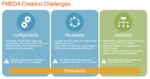
Figure 2 demonstrates the multiple challenges in creating FMEDAs.
Safety evaluation starts with a Failure Mode and Effect Analysis (FMEA) based on system design experience in the potential ways, causes and effects a system might fail. This becomes the starting point for a systematic FMEDA captured in reports for each component in a design. Listed for each failure mode is the potential impact on the system’s safety along with methods to prevent, detect and correct such breakdowns. Random failures, perhaps triggered through ionization by cosmic radiation, are of particular concern. The analysis is based on lengthy simulations of faults, determining how or if those malfunctioning behaviors propagate through the circuit.
FMEDA at a given level of design demonstrates rigor in planning and testing for failure modes at a detailed level. Moving up to the next level in the system design, FMEDAs are typically abstracted for aggregation into higher levels. Abstraction trims down the failure modes to those relevant to system analysis while preserving safety analysis coverage. Each use case drives the performance and may require building different abstractions during system-level analysis.
Within SoC design, the process suffers from scalability problems in three important ways, as highlighted in Figure 2. It is not designed to deal efficiently with highly configurable IP. The network-on-chip (NoC) provides a clear example. Each NoC configuration is unique to the designated SoC in the endpoint IPs it connects and quality of service and power goals. As the design changes prior to tapeout, so must the NoC. Each instantiation requires an independent analysis performed by the SoC integrator who knows the needed NoC configuration.
A natural question is whether at least some of this analysis could be reused between different configurations. Reuse is already successful in accelerating SoC design and plays a significant role in functional verification. In contrast, FMEDA is a relatively recent addition to design requirements and has yet to evolve a reuse strategy. Every analysis at a given level must be from scratch, consuming significant time and resources. A reuse strategy could make an enormous difference to design schedules and avoid errors if a solution was available.
The lack of a standard format for FMEDA is also an efficiency drain. SoC integrators using IPs from multiple suppliers must contend with different formats, requirements and assumptions on use-case compatibility and, therefore, other ways to derive abstractions. Today, these disconnects are resolved manually between integrators and suppliers, but the process is not scalable. There are too many points at which mistakes could occur.
Aligning FMEDA With Reuse
A reuse-centric methodology cannot be based on flat analysis at each stage. The essential failure modes of a configurable IP do not vary between configurations. These should be interpretable in parametric instantiations of the RTL, allowing the generation of an FMEDA for a particular layout. In this flow, failure modes and safety mitigation would be model-oriented rather than report-oriented. A model-based approach allows for generating and delivering an FMEDA model for an IP. The significant gain is that the SoC integrator no longer needs to run a full flat analysis for each configuration change during design development.
The next logical advance would be to extend this capability to SoC FMEDA build. A generator for an SoC-level analysis could read traditional FMEDA reports for IPs and apply in-context requirements and assumptions of use. This would optimize that detail down to a few essential failure modes relevant to that purpose per IP. The generator could then build the appropriate SoC FMEDA for that use model from this input. Generating a new analysis for a different set of assumptions would require no more effort than dialing in those new parameters and re-running the generator. Since the tool used is ISO 26262 certified, additional analysis is unnecessary before tapeout because the compliance is already built-in. Figure 3 illustrates the full proposed flow, from FMEDA generation at the IP level to FMEDA generation at the SoC level.
A methodology like this could greatly simplify safety analysis for an SoC development team, even if only one IP supplier endorsed the model-based capability. If each IP supplier supported a standard for safety data interchange, such as the IEEE P2851 standard currently in development, the value to the SoC safety analysis team would be amplified even further. Encouraging tooling to aggregate and abstract IP models for the SoC might depend more on the completion and adoption of IEEE P2851. However, given there are already solutions of this nature in some automotive SoC suppliers, this goal seems very achievable.
Traceability and FMEDA
Whenever requirements must be exchanged between integrators and suppliers, traceability becomes essential. The most important requirement in design for automotive applications is safety, as documented in the FMEDA. Requirements, implementation, testing and FMEDAs are closely interlinked. Changes in any of these must be correctly tracked in the others if the integrity of the whole process is to be maintained, as illustrated in Figure 4 below.
Figure 4 highlights that traceability between requirements, implementation, test and FMEDA is closely coupled.
There is another compelling reason to consider traceability here. At each level of integration, FMEDAs are abstracted from detailed structural-level failure modes to a much smaller number of system failure modes. This abstraction is performed based on use cases and system design experience. Mistakes are possible but can be mitigated through careful traceability from system failure modes down through component failure abstractions to more detailed component analyses.
Traceability is valuable for problem diagnosis and abstraction support against different use cases. An integrator may decide for one use case that certain failure modes are more important than others. Whereas in another situation, that decision might change. Given the ability to examine the full set of failure modes, an integrator can choose what to prioritize and ignore. With the support of a generator, as described in the previous section, an integrator would enjoy more flexibility to explore options.
A Call to Action
A move to reuse practices for FMEDA seems both logical and unavoidable. Reuse practices are already amply proven in design and verification. Now it is time for safety analyses to move up to that level. It would be natural also to align these interfaces with the planned IEEE P2851 standard as that starts to emerge. In the meantime, suppliers of highly configurable IP should craft solutions to better serve integrator customers. Automotive semiconductor solutions for aggregation and abstraction can help define a more complete solution at the SoC level. That approach must recognize the need for traceability through FMEDA.
Only through advances of this nature is it possible to jump past the looming problem in safety analysis scalability.
For more information about FMEDA, click HERE.
Mr. Stefano Lorenzini has more than 25 years of safe and secure SoC design and architecture experience spanning Arteris IP, Alcatel Microelectronics, Cadence Design Systems, Ericsson, Intel, ST Microelectronics, and Yogitech. He has spent the last 18 years managing SoC functional safety applications regulated by IEC 61508 and ISO 26262 standards. He holds a master’s degree in electronic engineering from the University of Pisa, Italy.
Also read:
Scaling Safety Analysis. Reusability for FMEDA


