Advanced semiconductor fabrication technology is what makes it possible to pack more and more transistors into a sq.mm of a wafer. The rapidly increasing demand for advanced-process-based chips has created huge market opportunities for semiconductor manufacturing equipment vendors. According to SEMI, worldwide sales of semiconductor manufacturing equipment in 2021 rose 44% to an all-time record of $102.6 billion. While the opportunities are big, delivering cost-effective equipment optimized for mass production involves overcoming a number of challenges.
In June 2022, SemiWiki published an article titled “Leveraging Simulation to Accelerate the Design of Plasma Reactors for Semiconductor Etching Processes.” That article was a brief introduction, leading up to a webinar on simulation techniques to accelerate design of plasma reactors for semiconductor etching processes. The webinar was presented by Richard Cousin of Dassault Systèmes and is now available on-demand for viewing. This article covers some salient points from that webinar.
Benefits of Simulation When Designing Plasma Reactors
Simulations help understand how a device will behave even before the device is actually manufactured. Whether the device being designed is a chip or a plasma reactor, the savings in terms of time and money is worth investing in a good simulation tool.
In the case of plasma reactors, the design has to balance many different parameters to accommodate various requirements and plasma characteristics. The plasma characteristics include the density profiles, the ionization rate, the effect of the pressure and the type of gas used as well as the influence of the geometry to prevent damages. Simulation can, for example, help experiment with different numerical and physical settings for a plasma reactor to improve uniformity of ion density profiles. It can also help perform thermal coupling analysis with the aim of eliminating vulnerabilities to reactor damage. It can also allow experimenting with different types of gases, pressures and power levels.
The benefits of simulation fall into three categories.
- Predicting and explaining experimental results, particularly when no diagnostics are available in advance
- Reducing cost of development by optimizing performance and reliability before actually manufacturing the plasma reactor (or modifying an existing reactor)
- Accelerating device validation and decision making on right manufacturing processes
Focus of Dassault Systèmes’ SIMULIA Tools
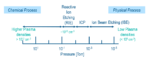
Depending on the pressure levels deployed, dry etching process would be a physical process or a chemical process. Refer to the Figure 1 below for the dry etching classification spectrum and the focus range of the spectrum for SIMULIA tools.
Figure 1: Dry Etching Process Classification as a function of the Pressure level
The anisotropic etching process is well suited for nanoscale size features. Also, more physical parameters can be controlled to characterize the plasma, such as the input power as well as the pressure of the neutral gas which controls the plasma density.
Simulation Techniques Deployed by SIMULIA Tools
The SIMULIA tools help analyze not only the steady-state model after the plasma is formed but also the transient model on how/when the plasma is formed. SIMULIA can use a microscopic approach or a macroscopic approach for the simulations.
Microscopic Approach
Under the microscopic approach, it uses a time-domain kinetic approach with a Poisson based Particle-In-Cell code to analyze space charge interactions. Several particle interactions are taken into account in a global Monte-Carlo Collision (MCC) type model. The ionization of the neutral gas, its excitation and the elastic collisions are considered simultaneously to compute the plasma kinetics.
Macroscopic Approach
Under the macroscopic approach, SIMULIA tools treat the plasma as bulk for RF plasma analysis and matching network optimization. Both linear and non-linear Drude dispersion models are available as options. This is well suited for use when designing Capacitive Coupled Plasma (CCP) type of reactors. With the application of a Bias Magnetic field, an Electric Gyrotropic Dispersion model is available for use when designing Inductive Coupled Plasma (ICP) type of reactors, for example.
SIMULIA Tool Use Cases
The SIMULIA tool can be used to simulate various types of plasma reactors. The following are three examples that were presented.
The DC Magnetron Sputtering Reactor Example
This design setup is as follows:
Pressure range: 1 to 5 mTorr
Target voltage: -400V
Target materials: Al, Cu or Ti
Target thickness: 1 mm to 3 mm
Goal: Estimating the target erosion profile for understanding long term sputtering efficiency
Figure 2 below shows the high correlation between the simulated results and measured results, as it relates to target erosion profile prediction.
Figure 2: Very good agreement between the predicted results and the experimental data for the Target erosion profile in a DC Magnetron Sputtering Device example
GEC CCP Reactor (Capacitive Coupled Plasma) Example
The design setup is as follows:
Pressure: 200 mTorr
Temperature: 300K
Gas: Argon neutral gas
RF-Voltage: 60V Peak-to-Peak
Discharge over 13.56MHz RF-Voltage
Goal: Control of plasma homogeneity
Figure 3 below shows the ion density profile as predicted by the simulator. This compares very well to density profiles presented in the technical literature for CCP reactors.
Figure 3: Well-known GEC Cell CCP Reactor. Ion Density Profile in good agreement with the published results for this Device
The VHF ICP Reactor (Inductive Coupled Plasma) Example
The design setup is as follows:
Pressure: 30 mTorr
Gas: Argon neutral gas
Input power: 300 W
EM-Field distribution: 13.56MHz
Goal: Characterize the physical parameters, understand the physical principles and identify potential issues and damages
Figure 4 below shows the plasma homogeneity issue and potential for damage from energy enhancement.
Figure 4: Electron Energy Enhancement localized which affects the plasma homogeneity and could lead to potential damage of the ICP Reactor