You are currently viewing SemiWiki as a guest which gives you limited access to the site. To view blog comments and experience other SemiWiki features you must be a registered member. Registration is fast, simple, and absolutely free so please, join our community today!
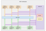
While Truechip has established itself as a global provider of verification IP (VIP) solutions, they are always on the lookout for strategic IP needs from their customer base. Over the last several years, a solid market for Network-on-Chip (NoC) IP has grown, driven by the need to rapidly move data across a chip. Concurrently, the TileLink interface specification has also been gaining broad adoption in SoCs for implementing cache-coherent transactions. This created a need for a NoC IP to work with the TileLink protocol. Truechip seized this opportunity last year and introduced their NoC Silicon IP that leverages the TileLink interface specification. An earlier SemiWiki post discussed Truechip’s NoC Silicon IP. While the TileLink specification was originally developed to work with the RISC-V architecture, it actually supports other instruction set architectures (ISAs) too.
Truechip’s NoC Silicon IP provides chip architects and designers with an efficient way to connect multiple TileLink based master and slave devices for reduced latency, power, and area. It also helps reduce physical interconnect routing and use of resources inside an SoC. Yet another constant demand in the chip world is the need for faster and more efficient verification of designs and IP. The ever increasing design complexities directly expand the scope of verification challenges for achieving full coverage. New verification methodologies are needed to increase the efficiency and efficacy of testing highly complex designs. Any level of automation that can be brought into the life of a verification engineer will help ease the burden, leading to faster creation of testbenches. Truechip has seized this opportunity to introduce some automation products to their customer base. Earlier this year, the company announced their Automation Products addressing NoC Verification and NoC Performance for revolutionizing the verification process.
NoC Automation Products
The different IP blocks not only need to work as per their internal specifications, they also need to interact at the system level. Verification requires checking how the various blocks interact against the specifications at the system level. Performing this task may involve manual calculations for checking against various latency requirements. Many times, this may also call for manually viewing signal waveforms. Truechip’s automation products help ease the task of verification engineers by mitigating these manual tasks, thereby reducing the time and effort needed for optimization. IP teams can more efficiently optimize their IP for maximizing bus and bandwidth utilization. Chip verification engineers and chip architects alike benefit from this automation.
NoC Performance Product
Truechip’s NoC Performance is a robust performance analyzer for NoC IP/SoC and supports fully compliant standard Bus interface ports like AXI, AHB, APB, and TileLink. It comes with compliance and regression test suites along with exhaustive set of assertions and coverage points. The product offers consistency of interface, installation, operation and documentation across all of Truechip’s VIP solutions.
Some Salient Features
Per interface latency and NoC latency
Latency variation over transactions
Transaction Tracing
Per interface bandwidth
Master and Slave Interface comparisons (in terms of bandwidth and Latency)
Consolidated summary timeline for different performance numbers in single window
Statistics for different types of commands encountered on bus Bandwidth (GBps) and throughput
Actual Data transfer
Time window to select the duration for computing utilization
Integration Guide, User Manual, FAQ, and Release Notes
NoC Verification IP
Truechip’s NoC Verification IP provides an efficient way to verify the components interfacing with any type of NoC IP or SoC. It is a light weight VIP with an easy, plug-and-play interface that minimizes the hit on design cycle times. The solution comes with a GUI based testbench generator (TBG) and supports fully compliant standard Bus interface ports such as AXI, AHB, APB and TileLink. The VIP is available in native System Verilog UVM and Verilog.
Some Salient Features
Automated Testbench creation & Integration of DUT and VIP
Automated Test case generation for sanity tests / full verification
End to end data score boarding
NoC Monitor
Regression running and analysis
Multiple protocols and (theoretically) any number of nodes
Integration Guide, User Manual, FAQ, and Release Notes
About Truechip
Truechip, the Verification IP specialist, is a leading provider of Design and Verification solutions. It has been serving customers for more than a decade. Its solutions help accelerate the design cycle, lowers the cost of development and reduces the risks associated with the development of ASICs, FPGAs, and SoCs. The company has a global footprint with sales coverage across North America, Europe and Asia. Truechip provides the industry’s first 24×7 support model with specialization in VIP integration, customization and SoC Verification.
This Diakopto paper discusses for the first time, a new effect – a false electrical mismatch in post-layout simulations for perfectly symmetric nets. This effect is caused by the difference in distributions of parasitic coupling capacitors over the nodes of parasitic resistor networks, even for symmetric nets. This, in turn, is caused by artifacts of parasitic extraction and parasitic extraction tools. Practical recommendations are proposed for identifying these false mismatch conditions, to distinguish them from real mismatches due to layout differences. Parasitic extraction methodology needs to be improved to avoid these artifacts and to ensure the trustworthiness of post-layout simulations and IC design flow.
Device and net matching in IC design
Many analog and RF integrated circuits rely on the concept of device and net matching [1,2]. Examples of such circuits are: StrongARM latch, sense amplifier, differential pair, current mirror, multi-phase clocks, and many others. Matched nets and devices allow a circuit to be more tolerant and insensitive with respect to unavoidable process variations.
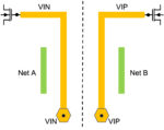
To enable perfect net matching, layouts are created symmetric (i.e. flipped around the X or Y axis), or by shifting or rotating a cell. An example of such symmetric nets is shown in Figure 1.
Figure 1. Layout of matched nets VIN and VIP. Input ports are VIN and VIP, and destination points are the gates of the MOSFETs. The nets and their environment are created symmetric, to ensure parasitic resistance, coupling capacitance, and RC delay matching.
A perfect symmetry and matching are rarely achievable, due to constraints of design rules, wire routability, and geometry. To verify matching, designers and layout engineers perform parasitic extraction, and then run post-layout circuit simulation – as a part of a standard post-layout design flow. If simulations show good and expected results, symmetry and matching have been achieved. If there are some offsets, mismatches, or differences in measured signals – it means the matching is not perfect, and the layout needs to be improved.
This methodology seems clear and straightforward, similar to a very basic, general concept of symmetry in physics. A symmetric system should possess a symmetry in its characteristics, and if its simulated or calculated characteristics are not symmetric – obviously, the solution is wrong.
Problem statement
However, very often post-layout simulations show difference(s) in electrical behavior even for perfectly symmetric, matched nets. A typical scenario is when two nets show a good matching for capacitance and for resistance, but a large mismatch for RC delay. At a first glance, it seems that the delays should match if capacitances and resistances are matched. So, the effect of delay mismatch, in such scenario, may seem counterintuitive.
Figure 2. (a) Visualization of parasitic elements – resistances and capacitances. Note the asymmetry, a difference in the distributions of coupling capacitances for nets VIN and VIP. (b) Visualization of RC delay over the net layout. Since coupling capacitances are concentrated at the far end (form the port VIN) of the net VIN, and at the near end of net VIP, the delay on VIN is larger than delay on VIP.
The root cause of the delay mismatch is related to how parasitic extraction tools distribute coupling capacitances over the nodes of the resistive networks. For some reason, the distribution of coupling capacitances is very asymmetric – different for symmetric (or for rotated) nets. This effect is illustrated in Figure 2. The most likely reason for such asymmetry is the anisotropy of computational geometry algorithms used by extraction tools, such as sweep (or scan) line, or polygon boundary traversing – which have a preferred direction, such as left-right, or top-bottom, or clockwise-counterclockwise. These algorithms are treating the layout as a flat system, losing the natural hierarchy and cell transformation characteristics, that, theoretically, can be used to transform the preferred directions according to cell transformations.
To prove (or disprove) this conjecture, we performed a series of experiments, by analyzing post-layout netlists and performing post-layout simulations for several GDS files. We used the original DSPF file (used as a reference), and compared with DSPF files obtained by various transformations – symmetry reflection with respect to the X and Y axes, and by rotations of 90, 180, and 270 degrees. The results for symmetry transformation are illustrated in Figure 3.
Figure 3. RC parasitic for the (a) original and (b) flipped GDS files. The distributions of coupling capacitances for nets VIN and VIP are reversed, for cases (a) and (b). The distributions of coupling capacitances are the same for the left net, and the same for the right net, for cases (a) and (b).
As one can see, the distribution of coupling capacitances is the same for the left net for the original and for flipped layout. This distribution is also the same for the right net. However, since nets VIN and VIP changed sides, for the flipped versus original layout, the distributions of coupling capacitance on net VIN (VIP) for case (a) now becomes the distribution of coupling capacitances for net VIP (VIN) for case (b).
This change in capacitance distributions correlated very well with the simulated RC delays on VIN and on VIP. RC delay is larger for net VIN than for VIP in case (a), but smaller than delay on VIP in case (b). Similarly, we observed a difference in post-layout circuit simulations, showing a significantly larger transition time for nets VIN in case (a), and smaller for case (b), than transition time on net VIP. This shows that the electrical mismatch between symmetric nets VIN and VIP is an artifact of parasitic extraction tools, as explained above.
Of course, if the difference in couplings and in RC delays for nets VIN and VIP does not change its sign after performing a transformation of the layout, such difference is caused by the real layout mismatch, and is a real effect, that needs to be fixed on the layout.
Coupling capacitors distribution over parasitic resistor network
To the best of our knowledge, this is the first paper discussing the artifacts of parasitic extraction related to anisotropic, asymmetric distribution of coupling capacitances for symmetric layout.
We observed these false mismatch effects for different designs, technologies, foundries, and for all three major parasitic extraction tools – StarRC, Quantus QRC, and Calibre PEX. The severity of false anisotropy is different for different extraction tools. This may be explained by a difference in the quality of coupling capacitors distributions, illustrated in Table 1 and Figure 4.
Table 1. Quality of coupling capacitance distribution for different parasitic extraction tools.
Every parasitic extraction tool tries to minimize the size of the parasitic RC network, to enable fast post-layout simulation times (for SPICE, EMIR, timing, and other tools). There is always a trade-off between the netlist size (simulation time) and accuracy. Different parasitic extraction tools do this with a different level of physics awareness, and with a different level of accuracy. Obviously, incorrect coupling capacitance distribution will lead not only to a mismatch between nets, but also to an inaccuracy in transient and AC simulations of such circuits.
Figure 4. Distribution of coupling capacitances over the nodes of parasitic resistor networks. Case (a) is the most accurate, case (b) is less accurate, and case (c) is very crude.
Advanced technology nodes (7nm, 5nm, 3nm, and beyond)
The false mismatch effect becomes much more severe in advanced technology nodes – such as 7nm, 5nm, and 3nm. Most likely, this trend is caused by a dramatic increase in parasitic resistances of interconnects for scaled technologies, which induces a bigger difference in RC delays for different RC distributions. Another reason is a relatively large contribution of parasitic capacitances to coupling capacitances and to RC delay (in addition to device intrinsic capacitances). A difference in distribution of parasitic coupling capacitances in advanced nodes may have a significantly bigger impact on RC delay mismatch for symmetric nets, than in older technologies (where device capacitance dominates). There may be other reasons, related to the behavior of parasitic extraction tools for advanced nodes, that is hidden from the users.
The algorithms adopted by parasitic extraction tools for coupling capacitance distributions are not discussed widely, and remain hidden from the users. There is not much control over this distribution in parasitic extractors commands and options.
Designs in advanced technology nodes are much more expensive than older nodes, in all aspects – engineering time, design, EDA tools, masks, manufacturing, wafer cost, time to tapeout, time to market, etc. That’s why false mismatches and their bigger impact in advanced nodes are much more critical and much riskier. People should start paying more attention to it – everyone, from designers and layout engineers to EDA tool vendors, to foundries, who qualify EDA tools and PDKs.
Simulation and analysis results
Post-layout SPICE simulation of a StrongARM latch [3] (see Figure 5) implemented in 5nm FinFET technology revealed a mismatch of transition times for devices M1 and M2 of ~500 fs, which was much higher than the upper limit spec for this mismatch (~30 fs). The layout was relatively small, and its visual inspection did not reveal any asymmetries. Designers and layout engineers did several iterations of the layout, trying to get rid of the mismatch in simulations – which took them over two weeks to do, without a success.
Flipping the layout around the Y axes resulted in a post-layout netlist that showed a mismatch with an opposite sign: –370 fs. This result is a clear, convincing argument that this mismatch of +500/-370 fs is caused by an artifact of the parasitic extraction tool.
Analysis of net mismatch using ParagonX™ EDA tool [4] confirmed a large RC delay difference of over 15% between nets in1 and in2 – with this difference changing its sign for the original and flipped layouts. Subsequent visualization of coupling capacitances using ParagonX further confirmed a strong asymmetry of their distributions. (These plots cannot be shown in this paper for third-party confidentiality reasons).
Figure 5. Schematic of StrongARM latch. Nets in1 and in2 should be matched for RC delay.
Interestingly, both resistances and net-to-net coupling capacitances for nets in1 and in2 were matched to a very high accuracy. Resistances were matched better than 0.05%, and coupling capacitances were matched better than 0.2%. This is a common effect we observed on many post-layout netlists – while capacitances and resistances on matched nets are very close, RC delays may be quite different, due to the effect discussed in this paper.
We believe that the 0.2% of capacitance difference is caused by the inaccuracy of rule-based (pattern-matching based) capacitance extraction. A much higher accuracy in capacitance extraction can be obtained using a random-walk based field solvers (FS), with a user-controlled accuracy goal settings. It is always recommended to use selected net FS extraction mode for nets whose capacitive matching (or binary or non-binary weighting – for capacitor array in SAR ADC) is critical for the circuit operation.
Discussion
Post-layout circuit simulation is considered a golden standard for analyzing and simulating custom, transistor-level IC designs. The observed false mismatch effect leads to an interesting question: how accurate is post-layout simulation? Obviously, post-layout simulation accuracy cannot be higher than the parasitic extraction tool accuracy. And while capacitance and resistance extraction is, in general, quite accurate, a crude distribution of coupling capacitances over the nodes of parasitic resistors network may lead to errors of ~500fs (or more) in transient and AC simulations. This finding may have important implications for the trustworthiness and accuracy of SPICE simulation for precision and high-speed analog designs, for timing analysis, and for other applications. As a minimum, the industry needs to establish a methodology for detecting, debugging, resolving, or getting around (see more on this in the next section).
Just as importantly, false mismatches, induced by extraction artifacts, may mask a real layout and electrical mismatch, caused by the differences in layouts and contexts of matched nets. Detecting a real mismatch becomes difficult or even impossible, in the presence of false mismatches. Also, a real mismatch may look like zero or small mismatch, if false and real mismatch coincidentally cancel each other – which is also a high-risk factor.
Practical recommendations
We can give the following recommendations:
1. For circuit designers and layout engineers:
a. Pay more attention to mismatches in general and to false mismatches caused by incorrect parasitic extraction in particular.
b. Increase the awareness of these effects. Request EDA tool vendors to improve the accuracy and get rid of such artifacts in parasitic extraction related to coupling capacitors distribution.
c. Use a field solver for accurate, controlled capacitance extraction of matched nets (if capacitance matching is critical).
d. Use ParagonX or scripts to proactively check and verify net and device matching in post-layout netlists, to debug such problems, and to improve the layout matching.
2. For EDA tool vendors: Improve the accuracy of parasitic extraction tools, and in particular, improve the quality of coupling capacitors distribution.
3. For foundries: Perform more thorough verification and qualification of parasitic extraction tools, related to net matching and to the quality of coupling capacitors distributions.
4. For EDA researchers: Come up with better algorithm and methodologies to improve the accuracy of post-layout netlists without exploding their size.
5. For all: Check for false mismatches in your design flow, introduced by parasitic extraction:
a. Create layouts by applying symmetry transformation to the original layout (see Figure 6), such as:
i. Flip around the X axis.
ii. Flip around the Y axis.
iii. Rotate by 180 degrees, and by 90 or 270 degrees (if DRC allows that).
b. Perform parasitic extraction.
c. Use ParagonX to compare post-layout netlists for original and transformed layout.
i. ParagonX detects / debugs mismatches much faster and easier than SPICE.
d. If ParagonX is not available, use post-layout SPICE simulation to compare two post-layout netlists; do STA analysis and comparison for custom digital.
e. In the case of significant differences, indicative of false mismatches:
i. Perform visual inspection of the layouts (if possible).
ii. Report findings to parasitic extraction tool vendors, and to foundries.
Figure 6. Layout transformations that can help identify a false net mismatch. Electrical characteristics are invariant with respect to these transformations, so parasitic capacitances, resistances, delays, devices, and SPICE simulations should be invariant as well.
Recommendations in section (5) above are based on a very basic, fundamental principle of symmetry in physics and mathematics – if a system possesses a certain symmetry, the characteristics of the system should display the same symmetry. The geometrical transformation symmetry of IC designs stems from the fact that circuit electrical characteristics are invariant with respect to these transformations.
Note that post-layout netlists for transformed layouts may have internal (non-port) nets, device instances, and instance pin names different from the original layout and netlist. Care must be taken when comparing transformed netlists, to make sure that the comparison is done on topologically identical objects (nets, instances, and instance pins).
It’s interesting, that to verify the accuracy of the parasitic extraction tool, we do not need another, more accurate, a golden reference tool – we can use the same tool, and see if it produces the same results for layouts that are rotated or flipped. Obviously, the RC delay should not depend on the orientation of the chip in space.
Feedback from the readers is welcome
Have you experienced or struggled with this or similar problems caused by IC layout parasitics? We welcome you to share your feedback, comments, suggestions, or frustration on parasitic effects, extraction tools, circuit implications, and layout debugging topics.
Maxim Ershovis a scientist, engineer, and entrepreneur. His expertise is in physics, mathematics, semiconductor devices, and EDA. Prior to co-founding Diakopto, Maxim was responsible for parasitic extraction at Apple’s Silicon Engineering Group. Before Apple, he was CTO of Silicon Frontline Technology, where he architected and successfully brought to market several industry-leading tools such as R3D and Rmap. Maxim also worked as device engineer at PDF Solutions, T-RAM Semiconductor and Foveon.
Prior to moving to the industry, he was a professor at Georgia State University and University of Aizu. Maxim graduated with a Ph.D. in Solid State Electronics from the Moscow Institute of Physics and Technology and won the first place in the Physics Olympiads (USSR) for high schools and for universities.
References
[1] “The art of analog layout”, 2nd ed., A. Hastings, Prentice Hall, 2005.
[2] “CMOS IC Layout: Concepts, Methodologies, and Tools”, D.Clein, Newnes, 1999.
[3] “The StrongARM Latch” (A Circuit for all seasons), B.Razavi, IEEE Solid-State Circuits Magazine, v. 7, no.2, p. 12-17, 2015.
The hand-wringing over Elon Musk’s takeover of Twitter began in earnest, Friday, as General Motors announced it would suspend advertising on the platform. Ford Motor Company, too, said it would take a step back.
The news of Musk’s completion of his Twitter acquisition completely eclipsed Mobileye’s hugely successful initial public offering and Ford and Volkswagen’s exit from their Argo.ai autonomous vehicle joint venture. But its relevance to both of those events is clear.
The concern across the automotive industry was that Musk will weaponize Twitter to advance Tesla’s electric vehicle market dominance – while downplaying competing voices and messages on Twitter. The pearl-clutching by GM seems pointless in a post-Truth world.
Musk, CEO of Tesla, has long been a liar of titanic dimensions. He’s lied about his personal and Tesla’s finances, lied about being a Tesla founder, lied about the current and future performance of Tesla vehicles, lied about selling Tesla, lied about taking Tesla private.
Lying is what Musk does best. And he is in good company.
Liars are extremely popular on social media – from Twitter and Meta/Facebook to Instagram, Tik Tok, Whatsapp, and Snapchat. The most popular posters are paid influencers for whom sponsored lying is their stock in trade.
Elsewhere, compromised commentary is driven by stock ownership with critics holding short positions and fans touting stocks they own – without disclosing that ownership. It’s impossible to get a straight story.
In the “news”-infused world we live truth is an orphan. This is one of the reasons I tend to eschew auto shows. Auto shows represent the pinnacle of paid messaging. The straight dope, the skinny, is not invited to the auto show – though the press is present in force.
In this context, it is utterly amusing that any marketing or communication executive in the automotive industry would be raising red flags over Musk potentially bending Twitter to his will. Marketers have been working diligently to bend all social media platforms to their marketing will. Musk has simply taken ownership of one of those platforms.
Make no mistake. We live in a post-Truth world.
Scanning the headlines across the full range of news and information sources available physically and online puts one in the position of Diogenes – holding a lantern to the faces of the citizens of Athens seeking an honest man. Is anyone honest anymore? Was anyone ever honest?
Whether in pursuit of political news or even movie reviews, nearly every source of information and insight has been co-opted and corrupted. Opinions are regularly bought and paid for. Influence is the coin of the realm and available for a price.
Musk is the master of the marketing masque. Tesla has been shipping cars with lousy build quality for years and charging for a Full Self Driving feature – that does no such thing – and getting away with it.
Regulators, politicians, consumers, competitors, law enforcement – no one has been able to stop Musk. Now, as CEO of Twitter, he is perched atop the social media demimonde in full-self-aggrandizing mode.
In this context, it is no surprise that Ford and Volkswagen chose to terminate their own self-driving venture Argo.ai. Argo.ai was headed by Bryan Salesky, a former Google executive who assiduously avoided the spotlight.
Salesky loathed the demands of marketing and messaging regarding the work of Argo.ai. He refused to be lured into the trap of spinning a Musk-like yarn regarding Argo.ai’s progress for the public or investors.
Salesky’s unwillingness to participate in the autonomous vehicle marketing moshpit sadly doomed Argo.ai. Diogenes might have approved of Salesky, but investors did not.
The message for us all in a fake-it-til-you-make-it world is the need to embrace the dissembling and exaggeration to spin up public enthusiasm and deceive investors in order to achieve success. No one seeks honesty on Twitter. No one ever did. The least we can do in a world where so many are seeking to deceive us is try hard not to deceive ourselves.
Dan is joined by Barry Paterson, CEO of Agile Analog. Barry has held senior leadership, engineering and product management roles at Wolfson Microelectronics and Dialog Semiconductor. He has been involved in the development of custom mixed-signal silicon solutions for many of the leading mobile and consumer electronics companies across the world. He has a technical background in Ethernet, audio, haptics and power management and is passionate about working with customers to deliver high quality products.
Barry provides an overview of exciting new development at Agile Analog, including new technology and new analog IP titles, as well as a unique digital cell library that is well-suited to digital control of analog processing.
The views, thoughts, and opinions expressed in these podcasts belong solely to the speaker, and not to the speaker’s employer, organization, committee or any other group or individual.
As more AI applications turn to edge computing to reduce latencies, the need for more computational performance at the edge continues to increase. However, commodity compute engines don’t have enough compute power or are too power-hungry to meet the needs of edge systems. Thus, when designing AI accelerators for the edge, Joe Sawicki, the Executive VP for the IC EDA Division of Siemens, at last month’s AI Hardware Summit in Santa Clara, Calif., suggests that there are several approaches to consider: Custom hardware that is optimized for performance, high-level synthesis to radically reduce design cost, and hybrid verification to significantly reduce validation cost.
When these approaches are combined, designers can craft high-performance AI accelerators for edge computing applications. That high performance will be needed since model sizes of the AI algorithms are growing over time—over the past five years, explained Sawicki, the models (such as the ImageNet algorithm) have increased in computational load by more than 100X and that growth shows no sign of slowing down.
Industry estimates from International Business Strategies show that the AI value contribution to the overall IC market revenue will grow from today’s 18% to 66% by the year 2030, while the total IC market revenue will grow from $529 billion today to $1144 billion by 2030. The gain in AI value demonstrates the increasing momentum in custom accelerators to improve both edge device performance and overall AI performance. Although the customized accelerators can deliver exceptional performance, they have one drawback – they have limited flexibility since they are typically optimized for a limited number of algorithms.
In an example described by Sawicki, a configurable block of AI intellectual property is compared to a custom AI accelerator design. Area, Speed, Power, and Energy all show significant reductions for the custom accelerator (see table). For example, area is 50% smaller, speed improved by 94%, power dropped by 60%, and energy consumed per inference was reduced by 97%. It’s not magic here–it’s because the architecture was specifically targeted to implement the specific algorithm explained Sawicki.
Part of the optimization challenge is to determine the best level of quantization—for example, 32-bit floating-point accuracy is often preferred, but with just a small loss in the result precision, a 10-bit fixed-point alternative that saves 20X in area/power can be used instead, thus improving compute throughput and reducing chip area. Additionally, by applying high-level synthesis in the hardware design flow, designers can go from the neural network architecture to a C++ bit-accurate algorithm to a C++ Catapult architecture and on to high-level synthesis to craft a synthesizable RTL design that can be implemented using RTL synthesis tools and back-end tool flows.
The use of C++ allows designers to easily explore various architectural approaches, suggests Sawicki. In a second example, he described the design exploration of a RISC-V Rocket core and three design options in a 16-nm process—one that is optimized for low power using an accelerator plus the Rocket core, a second that focused on shrinking the core area to minimize silicon cost, and a third approach that was optimized for speed. For the low-power option, the core plus accelerator consumed 86.54 mW, ran at 25.67 ms, and occupied a total area of about 3 million square microns. The second option reduced the total silicon area by about one-third to 2 million square microns, slowed down the execution to 37.54 ms, and kept the power to just under 90 mW. Lastly, the speed optimized version upped the area back to about the same level as the first option, improved the speed to just 12.07 ms, but upped the power consumption to 93.45 mW. These tradeoffs show that design choices can considerably affect the performance and area of a potential design.
The incorporation of AI/ML function in an EdgeAI design also adds additional verification challenges. The verification tools must deal with the training data set, the AI network mapping, as well as the AI accelerator logic (the structured RTL). As Sawicki explained, functional benchmarking has to deal with virtual platform performance, modeling of the hybrid platform, and simulation/emulation of the modeling platform. And all through that the tools must also perform power and performance analysis. To do that, the verification technology has to be matched to the needs of the project—hybrid verification and run-fast/run-accurate (ability to switch between model fidelity in a single run) make it possible to test real-world workloads in the verification environment.
By using open standards Sawicki expects designers to leverage a rich ecosystem of modeling capabilities in a heterogeneous environment for multi-domain and multi-vendor modeling. Tools for scenario generation, algorithmic modeling, TLM modeling and physics simulations can all be tied together via a system modeling interconnect approach that allows analog and digital simulation, hardware assisted verification through the use of digital twins, and virtual platform models to interact.
SemiWiki recently posted a blog on “Deep Data Analytics for Accelerating SoC Product Development.” That blog focused on proteanTecs’ AI-enabled chip analytics platform that helps accelerate SoC product development. The blog provided insight into proteanTecs’ approach and shared quantifiable business-impact metrics as derived by Semico using a sample data center accelerator SoC.
proteanTecs recently published a whitepaper on how to enhance the economics of testing by leveraging its solution together with Advantest’s Advanced Cloud Solutions (ACS) Edge solution. With proteanTecs delivering enhanced visibility through embedded Universal Chip Telemetry (UCT), the ACS Edge enables the production test environment for real-time execution. The combination elevates production testing to a new level. This post will discuss the salient points garnered from that whitepaper.
Challenges for Enhanced Testing
With the ever increasing levels of system integration, the following are some of the Testing challenges.
Applications involve increasing amounts of hardware-software interactions, whether it is mobile oriented products or other embedded products
Ever increasing levels of integration within the same physical constraint makes it hard to understand the operating conditions at failure
Difficulty correlating results across test, assembly and system integration stages, due to lack of a common data language
Lack of visibility into operating conditions leading up to a failure, thereby making root cause analysis (RCA) difficult
Gaps in Current Testing Approaches
Traditionally, each stage of testing from post-silicon validation to system level testing has been with different equipment using different data languages for describing the respective tests. While the segmented approach may have helped optimize each stage, overall results could fall short of what is achievable through an integrated approach. As the segmented approach lacks data sharing among different testing stages, optimizing product cost is difficult. An overall optimization workflow with data sharing is needed for effective and economically efficient testing.
Moving Coverage Between Stages
Wafer Test has the highest cost per second, followed by Package Test and then System Level Test (SLT). But in order for a device manufacturer to guarantee the field failure rate, all that matters is the quality and reliability of the final product. As a device moves through different stages, the test cost vs cost of scrapping a device changes, directly impacting the profitability of a product. Naturally, a device manufacturer would want to run all of the effective screens at the earliest point, saving only elusive faults for system level testing.
For example, $500K of scrap costs may have been avoided by moving 5% coverage from package test to wafer sort. In order to shift-left or shift-right some coverage, one must correlate if the test at one stage is equivalent to the test at another stage. But that decision to move can only be enabled through improved visibility into each stage, allowing tests to be adjusted for each test insertion.
proteanTecs Platform
proteanTecs platform is designed to provide detailed device visibility from initial manufacturing testing throughout the device’s lifetime. It is a holistic software platform that applies machine learning and analytics to data created by on-chip UCT agents. The platform’s pre-configured set of dashboards provide meaningful and useful insights and alerts. The platform is scalable and flexible and fuses information from the entire fleet of chips and systems. And, it offers an open development environment for incorporation of customized algorithms.
Advantest’s ACS Edge™ Platform
Advantest’s ACS Edge™ is a high performance, highly secure edge compute and analytics solution enabling ultra-fast algorithmic AI decision making with millisecond latencies during test execution. ACS Edge connects to test equipment via a private high-speed encrypted link. Users develop machine learning or other compute-intensive applications which operate near real-time on data generated by tests in the test program. These applications are wrapped in an Open Container Initiative (OCI) compliant container which simplifies global distribution and management while hardening them against compute environment changes.
proteanTecs + ACS Edge: Tremendous Potential
The combination of the proteanTecs analytics platform with the ACS Edge analytics solution offers tremendous potential to change the economics of testing. Compared to traditional testing approaches, the combined solution delivers the following benefits.
Reduced test execution time (more than 70% reduction compared to traditional approaches)
Production yield improvement (more than 2% compared to traditional approaches)
Enhanced outlier detection within an insertion
Real-time adaptive test
Reduction in retesting
Improved visibility for shift-left decisions
The whitepaper includes lot of examples and use cases with benefits achieved reported in quantified form. For full details, download the joint whitepaper.
Area selective processing (ASP) is assuming ever greater importance in semiconductor fabrication. ASP involves deposition and removal of materials at the molecular level¾10 nm or less. Key applications of ASP include self-aligned contacts and fully self-aligned vias (FSAVs), scaling boosters that are essential to continue device shrinkage. By supporting techniques like metal-recess flows and dielectric-on-dielectric (DoD) flows, ASP can provide the tools needed for the semiconductor industry to stay on the roadmap.
Executing these precision fabrication steps requires very tight control of deposition and etch. These are complex processes with challenging chemistries. By addressing those issues, EMD Electronics, a business of Merck KGaA, Darmstadt, Germany, and its integrated portfolio of companies, provides a complete solution that enables semiconductor companies to build innovative devices.
Paths to ASP
Just as different types of photoresists have been formulated for conventional wafer patterning, so different ASP approaches have been developed to perform different tasks in additive fabrication.
· Intrinsically Selective Molecules
Intrinsically selective molecules are molecules engineered to aggregate on specific materials, such as metals only or dielectrics only. They can be used for selective deposition or for selective epitaxial growth. Applications include the growth of silicon germanium (SiGe) source/drains for logic or memory transistors, or Si/SiGe stacks for nanosheet gate-all-around (GAA) transistors.
· Small-Molecule Inhibitors
As the name suggests, small-molecule inhibitors discourage molecules from depositing on a surface. They are typically used to prepare nonplanar surfaces for the pattering of very small structures. The approach enables more aggressive scaling of design rules, which might otherwise be limited by gate-to-source/drain spacing and metal fill.
· Self-Assembled Monolayers
Self-assembled monolayers (SAMs) can be spun on or applied using vapor-phase deposition. These precisely assembled layers are used for selective capping of the top or bottom of fine structures such as lines and spaces or vias. SAMs enable bottom-up fill of advanced-node trenches or vias.
· Atomic-Layer Etching
Being able to precisely remove material is just as important as being able to precisely deposit it. Atomic-layer etching (ALE) enables the removal of monolayers of material. Applications include thickness reduction of DRAM dielectrics and cleanup steps like reactive ion etching (RIE). Atomic-layer etch is also used to create SiGe recesses in GAA transistors or to etch away other metal recesses.
EMD Electronics participates in all these areas.
ASP in action¾fully self-aligned vias (FSAVs)
FSAVs provide a good example of how ASP is being used to support device scaling. FSAVs are vias aligned with lines during the fabrication process through successive deposition and etch. It’s an effective approach but depends upon accurate positioning. Beyond the 3-nm node, edge placement errors (EPEs) from one layer to the next can be a problem. Now, the via is too close to the adjacent line. In extreme cases, copper can diffuse to the adjacent line, causing a short.
Reducing the width of the via in the next layer can help prevent this but the trade-off is increased resistance, with heat generation and greater power consumption, as well as RC delay. The alternative is to widen the spacing. This can be done in one of two ways: metal-recess flow and dielectric-on-dielectric (DoD) flow.
Metal-recess flow is an ASP step based on precision removal. It begins post CMP with a highly controlled etching step to create recesses in the copper (see figure 1). A second precision etch step cleans up the slides of the barriers down to the dielectric. Finally, the next layer of copper is deposited. The metal recess step increases the spacing between the via and the adjacent line.
Figure 1: Edge placement errors (EPEs) that reduce spacing between vias and adjacent lines can enable copper to diffuse across to the adjacent line, causing a short. In metal-recess flow, recessing the copper lines increases the distance between the via and the interconnect (right), preventing diffusion.
The DoD flow process requires both precision deposition and precision removal. In the DoD flow process, an inhibitor SAM engineered to grow on the copper but not the dielectric is grown on the metal (see figure 2). Next, a dielectric layer is deposited on the existing dielectric¾but the inhibitor layer prevents the growth of dielectric on the copper. After deposition, the inhibitor layer is removed from the copper. The cycle finishes with the growth of the next layer of via. Once again, the spacing between the via and the adjacent line has been increased using ASP.
Note that the dielectric-on-dielectric layer remains even after removal of the inhibitor layer.
Figure 2: In the DoD flow process, a copper-selective inhibitor (gray) is grown on the copper (brown). These features make it possible to deposit a dielectric layer (green) on top of the existing dielectric (blue). Once the inhibitor is removed from the copper, the next layer of via is deposited. Once again, the space between the via and the adjacent line is extended.
The fully self-aligned via (FSAV) process with ASP presents a few challenges:
DoD Process:
Materials: Developing a SAM selective for copper
Process conditions: High temperatures can degrade SAM molecules, but atomic-layer deposition (ALD) traditionally yields the best quality dielectric thin films at higher temperatures.
Chemistry: The halogen and oxygen precursors typically used for silicon dioxide (SiO2) ALD can damage the SAM, so we need halogen-free precursors and milder oxidants such as water.
ALE of copper is a multistage process requiring complex chemistry. The first stage involves chemically modifying the copper. The second stage actually removes the modified copper.
EMD Electronics has the answers
We specialize in sophisticated chemistries and can draw on the resources of our integrated solutions across the organization. This has enabled us to solve the core challenges across the process.
Materials: We’ve developed a SAM molecule that is copper selective.
Process conditions and chemistry: We’ve developed a reduced-temperature ALD based on a halogen-free silicon precursor with water as the oxidant. Despite running at lower temperatures, the process yields high quality dielectric films (dielectric constant ≤ 5; leakage current ≤ 5e-7A/cm2), without damaging the SAM molecules.
DoD Selectivity: as a result of the above-mentioned material and process development, we are able to demonstrate selectivity of deposited SiO2 film up to ~10nm for deposition on SiO2 and minimal, if any, deposition on copper (figure 3)
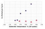
Chemistry: By optimizing the molecular composition of the chemistry and the copper modification stage of our ALE process, we have demonstrated effective and highly controlled copper removal with minimal added roughness. This is an important improvement over conventional processes, that allowed for atomic level control over copper etch rate (see figure 4).
Figure 3: DoD selectivity of >95% for deposited SiO2 film upto thickness of ~10nm on SiO2 but not on copper (Ref. G. Liu et al., ASD 2022 Conference)
Figure 4: Atomic level control over copper removal using our optimized ALE (blue) process , beginning at 170° C. Conventional ALE (pink) shows minimal removal of copper, regardless of process temperature.
Conclusion
ASP is an essential technology to equip the semiconductor industry to meet the challenges of the future. We used FSAVs here to highlight the power of ASP and our technologies but there are many other applications for this suite of processes in the semiconductor industry. ASP can be used for selective metal definition for source/drain. They can be applied to create an area-selective copper line barrier, for example, or for metal-on-metal deposition, such as a cobalt cap.
EMD Electronics supports the full ASP process, from the SAMs required to protect the surface to the precursors of processes required to deposit materials at low temperatures to the specialty processes needed to etch away inhibitors. We have novel chemistries to address the challenges. We have processes and chemistries optimized to work together. Most of all, we have an organization that delivers vertically integrated support for development, problem-solving and innovation.
Dan is joined by Sagar Pushpala, a seasoned semiconductor professional with more than 35 years of experience with IDMs, fabless and related semiconductor entities. He is actively involved with nearly a dozen companies in the US, Singapore and India in advisory/board, consulting and investment roles.
Dan explores the dynamics of the worldwide semiconductor ecosystem with Sagar. Potential mergers, consolidation, areas requiring more investment and the interplay between financial and political forces are all discussed with specific comments for all regions of the world.
The views, thoughts, and opinions expressed in these podcasts belong solely to the speaker, and not to the speaker’s employer, organization, committee or any other group or individual.
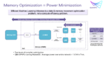
In wearables and hearables, low power is king. Earbuds for example still only manage a half-day active use before we need to recharge. Half a day falls short of truly convenient for most of us – a full day would be much better, allowing for overnight recharge. Physics limits battery sizes so system designers must look to SoC architectures to reduce power further. BLE is the obvious choice for communication with a nearby phone or other device but is a minimum requirement; further extending battery life requires more ingenuity. Some will come from cleverness in software running on an MCU or DSP, managing sensing, audio, automatic noise reduction and gesture recognition. However one significant opportunity is often overlooked – power reduction through application-specific SRAMs.
Why look to SRAMs for power reduction?
Embedded SRAM compilers provide some help in managing power, though typically fairly coarse-grained. Memory compiler vendors have consolidated significantly and together with foundry IP services must serve a broad range of market needs. Those providers can’t optimize for every possibility; instead, they tune for most popular options. Any design with an application-specific requirement must make do with a close but probably less than ideal fit. Second, all competitors have access to the same compilers. Since a significant percentage of a power budget consumed is likely in embedded memory, using a mainstream memory is a missed opportunity to differentiate on power.
Is it really possible to do better than the standard compilers? Dynamic power control in a memory doesn’t work the same way as in logic. Standard compilers offer a variety of compile options which primarily control the periphery and array-wide power switching. One way to go deeper while still using standard bitcells is to augment standard memory architectures. Clever address coding, limiting long line voltage swings and better control of bitline voltage swings are possible techniques here. For leakage, support for multiple banks allows for independent control of each bank and bitline control can also reduce leakage. Together these options can contribute significant power saving, both dynamic and static.
Going lower
Another familiar way to reduce power is to reduce voltage in DVFS operation. Here again, the constraints for memory are a little different than those for logic. The lower bound is the minimum voltage at which a memory cell can retain its value – Vret. However, the lowest voltage at which that memory content can be reliably accessed – Vmin – is normally close to the nominal operating voltage. A memory design which could drop Vmin closer to Vret could deliver significant power saving thanks to the V2 factor in dynamic power.
sureCore memory solutions
sureCore, based in the UK, has built application specific compilers for low power memories taking advantage of such ideas. One product, PowerMiser, offers single port SRAM IP with programmable sleep modes. PowerMiser delivers up to 50% dynamic and 20% static power reduction over competing options and is available as a compiler or in single instances. EverOn is the ultra-low power option, supporting operating voltages as low as Vret. In banked memory, a single bank can be powered at this low level to support wake functionality while other banks are powered off. This option is also available in compiler and single instance options. EverOn has shown 70% reduction in dynamic power and 60% in leakage power.
Another product line, MiniMiser, builds register files tuned to application-specific needs. The single rail design is not based on foundry bit cells and can be connected directly to system logic. MiniMiser memories commonly deliver power savings of >50% over competing options and are typically delivered as instances.
Not magic but careful design
How is sureCore able to offer these advantages? They build their own memory architectures, their own compilers and in some instance their own bit cells, guided by discussions with customers and their system application needs. They have also built their own automation for verification and robust characterization. Paul Wells, the CEO tells me that in many instances sureCore see common themes, around wearable, around AI, and around other applications. These drive in some cases standardized compilers, though they also advise clients on how to optimize configurations to system needs. Discussions might examine factors such read versus write dominance in an application for example.
In cases where a client needs the best possible power profile, sureCore offer a custom program called sureFIT. Here they work with a client using every trick in the book to build a one-of-a-kind solution. Techniques here include segmented arrays and bit-line voltage control, near-threshold operation, pipelined read circuitry and more.
sureCore memories already has deployments in several wearable, AI and RISC-V applications. You should check them out. As an IP service provider ranging between standard solutions and bespoke options to deliver best-in-class power profiles for many edge applications, sureCore is an intriguing proposition. It will be interesting to see how their business evolves!
Performance, Power and Area (PPA) are the commonly touted metrics in the semiconductor industry placing PPA among the most widely used acronyms relating to chip development. And rightly so as these three metrics greatly impact all electronic products that are developed. The degree of impact depends of course on the specific electronic products and the target end markets and applications. Accordingly, PPA tradeoff decisions are made by product companies when choosing the various chips (and IP for ASICs) for their respective end products.
Yet another important consideration has to do with ensuring a product’s longevity without requiring a redesign. In other words, future proofing one’s product against changing market/product requirements. While product companies deploy auxiliary ways to extend the life of a product before having to redesign, the path that offers direct future proofing is the preferred one. For example, FPGAs played a key role in future proofing communications infrastructure oriented products during the market’s aggressive growth period with fast changing requirements. Sure, an alternate path may have offered better PPA benefits than the FPGA path delivered. But the FPGA path helped the product companies save lot of time and money by avoiding redesign/re-spin of chips and ensured they were able to maintain/grow their market share.
An additional consideration is the path that offers ease and speed at which a product could be developed. This directly translates to time to market which translates to market share and profitability. And last but not least is the ease with which customers could develop applications software on the product.
Market Situation
Artificial Intelligence (AI) driven, machine learning (ML) enabled products and applications are fast growing with enormous market growth opportunities. New ML models are being introduced in rapid fashion and existing models are being enhanced as well. The market opportunity spectrum ranges from data centers to edge-AI products and applications. Many of the products targeting these markets cannot afford to tradeoff PPA against future proofing against ease of product/application development.
What if there is a way to offer PPA optimization, future proofing, ease of product development and ease of application development, all rolled into one offering? A hybrid processor IP that simplifies SoC hardware design and programming. An unified architecture that addresses ML inference, pre-processing and post-processing all-in-one.
New Category of Hybrid SoC Processor
Recently, Quadric announced the first family of general-purpose neural processors (GPNPUs), a semiconductor intellectual property (IP) offering that blends neural processing accelerator and digital signal processor (DSP). The IP uses one unified architecture addressing ML performance characteristics and DSP capabilities with full C++ programmability. This post will look at the components of a typical ML-enabled SoC architecture, its limitations, the Quadric offerings, benefits and availability information.
Components of a Typical ML-Enabled SoC Architecture
The key components of a ML-enabled architecture include the neural processing unit (NPU), the digital signal processing (DSP) unit and a real-time central processing unit (CPU). The NPU is used to run the graph layers of today’s most popular ML networks and performs very well on known inference workloads. The DSPs are used to efficiently execute voice and image processing and involve complex math operations. The real-time CPU is used for coordinating ML workloads between the NPU, DSP and the memory that holds the ML model weights. Typically, only the CPU is directly available to the software developer for code development. The NPU and DSP are accessible only through pre-defined application programming interfaces (APIs).
Limitations of a Typical Architecture
As mentioned above, the typical accelerator NPUs are not fully programmable processors. While they run known graph layers very efficiently, they cannot run new layers as the ML models evolve. If a ML operator not available through an API is needed, it would need to be added on the CPU, knowing that it will perform poorly. The architecture does not lend itself to future proofing for new ML models and ML operators. At best, lower performing solutions can be rendered by implementing new ML operators on the real-time CPU.
Another limitation is that programmers have to partition their code across the NPU, DSP and real-time CPU and then tune the interactions for meeting the desired performance goals. The typical architecture may also lead to splitting matrix operations between a NPU core and a CPU core. This action leads to inference latency and power dissipation issues as large data blocks need to be exchanged between the cores.
Multiple IP cores from various IP suppliers force developers to rely on multiple design and productivity tool chains. Having to use multiple tool chains generally prolongs development times and makes debugging challenging as well.
Benefits of The Quadric Approach
Quadric’s Chimera GPNPU family creates a unified, single-core architecture for both ML inference and related conventional C++ processing of images, video, radar and other signals. This allows for the neural network graphs and C++ code to be merged into a single software code stream. Memory bandwidth is optimized by a single unified compilation stack and leads to significant power minimization. Programming a single-core system is also a lot easier and preferred than dealing with a heterogeneous multi-core system. Only one tool chain is required for scalar, vector, and matrix computations.
Other benefits of the unified Chimera GPNPU architecture include area and power savings resulting from not having to shuffle activation data between the NPU, DSP and CPU. The unified core architecture greatly simplifies hardware integration and makes the task of performance optimization much easier.
The system design task of profiling memory usage to determine the optimal amount of off-chip bandwidth is simplified as well. This also directly leads to power minimization.
Application Development
The Chimera software development kit (SDK) allows for the merging of graph code from common ML training toolsets with customers’ C++ code through a two-step compilation process. This leads to a single code stream that can run on the unified Chimera single processor core. The widely used ML training toolsets supported are TensorFlow, PyTorch, ONNX, and Caffe. Users of the implemented SoC will have full access to all of Chimera core resources for maximum flexibility with applications programming. The entire system can also be debugged from within a single debug console.
Future Proofing Without Losing Performance
The Chimera GPNPU architecture excels at convolution layers, the heart of convolutional neural networks (CNNs). Chimera GPNPUs can run any ML operator. Custom ML operators can be added by writing a C++ kernel utilizing the Chimera Compute Library (CCL) API and compiling that kernel using the Chimera SDK. The custom operators are performant at the native operators’ level as they utilize the relevant core resources of the Chimera GPNPU.
SoC developers can implement new neural network operators and libraries long after the SoC has been taped out. This in itself increases a chip’s useful life dramatically.
Software developers can continue to optimize the performance of their models and algorithms throughout a product’s lifecycle. They can add new features and functionality and gain a competitive edge for their products in the market place.
Current Offerings from Quadric
The Chimera architecture has already been proven at-speed in silicon. The entire family of QB Series GPNPUs can achieve 1 GHz operation in mainstream 16nm and 7nm processes using conventional standard cell flows and commonly available single-ported SRAM. The Chimera cores can be targeted to any silicon foundry and any process technology.
The QB series of the Chimera family of GPNPUs includes three cores:
Chimera QB1 – 1 trillion operations per second (TOPS) machine learning, 64 giga operations per second (GOPs) DSP capability
Quadric is ready for immediate engagement with customers.
November 2022: Beta release of Quadric’s SDK.
Q1, 2023: Full production release of Quadric’s SDK
End of Q1, 2023: Production ready RTL of Quadric’s GPNPU IP
About Quadric.io
Quadric.io Inc. is the leading licensor of general-purpose neural processor IP (GPNPU) that runs both machine learning inference workloads and classic DSP and control algorithms. Quadric’s unified hardware and software architecture is optimized for on-device ML inference. Learn more at www.quadric.io.