

For many years, monolithic chips defined semiconductor innovation. New microprocessors defined new markets, as did new graphics processors, and cell-phone chips. Getting to the next node was the goal, and when the foundry shipped a working part victory was declared. As we know, this is changing. Semiconductor innovation is now driven by a collection of chips tightly integrated with new packaging methods, all running highly complex software. The implications of these changes are substantial. Deep technical skills, investment in infrastructure and ecosystem collaboration are all required. But how does all of this come together to facilitate the invention of the Next Big Thing? Let’s look at how TSMC redefines foundry to enable next-generation products.
What Is a Foundry?
The traditional scope of a foundry is wafer fabrication, testing, packaging, and delivery of a working monolithic chip in volume. Enabling technologies include a factory to implement a process node, a PDK, validated IP and an EDA design flow. Armed with these capabilities, new products are enabled with new monolithic chips. All this worked quite well for many decades. But now, the complexity of new product architectures, amplified by a software stack that is typically enabling AI capabilities, demands far more than a single, monolithic chip. There are many reasons for this shift from monolithic chip solutions and the result is a significant rise in multi-die solutions.
Much has been written about this shift in the innovation paradigm it enables. In the interest of time, I won’t expand on that here. There are many sources of information that explain the reasons for this shift. Here is a good summary of what’s happening.
The bottom line of all this is that the definition of product innovation has changed substantially. For many decades, the foundry delivered on the technology needed to drive innovation – a new chip in a new process. The requirements today are far more complex and include multiple chips (or chiplets) delivering various parts of the new system’s functionality. These devices are often accelerating AI algorithms. Some are sensing the environment, or performing mixed signal processing, or communicating with the cloud. And others are delivering massive, local storage arrays.
All this capability must be delivered in a dense package to accommodate the required form factor, power dissipation, performance, and latency of new, world-changing products. The question to pose here is what has become of the foundry? Delivering the enabling technology for all this innovation requires a lot more than in the past. Does the foundry now become part of a more complex value chain, or is there a more predictable way? Some organizations are stepping up. Let’s examine how TSMC redefines foundry to enable next-generation products.
The Enabling Technologies for Next Generation Products
There are new materials and new manufacturing methods required to deliver the dense integration required to enable next-generation products. TSMC has developed a full array of these technologies, delivered in an integrated package called TSMC 3DFabric™.
Chip stacking is accomplished with a front-end process called TSMC-SoIC™ (System on Integrated Chips). Both Chip on Wafer (CoW) and Wafer on Wafer (WoW) capabilities are available. Moving to back-end advanced packaging, there are two technologies available. InFO (Integrated Fan-Out) is a chip-first approach that provides redistribution layer (RDL) connectivity, optionally with local silicon interconnect. CoWoS® (Chip on Wafer on Substrate) is a chip-last approach that provides a silicon interposer or an RDL interposer with optional local silicon interconnect.
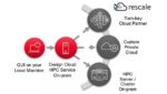
All of this capability is delivered in one unified package. TSMC is clearly expanding the meaning of foundry. In collaboration with IP, substrate and memory suppliers, TSMC also provides an integrated turnkey service for end-to-end technical and logistical support for advanced packaging. The ecosystem tie-in is a critical ingredient for success. All suppliers must work together effectively to bring the Next Big Thing to life. TSMC has a history of building strong ecosystems to accomplish this.
Earlier, I mentioned investment in infrastructure. TSMC is out in front again with an intelligent packaging fab. This capability makes extensive use of AI, robotics and big data analytics. Packaging used to be an afterthought in the foundry process. It is now a centerpiece of innovation, further expanding the meaning of foundry.
Toward the Complete Solution
All the capabilities discussed so far bring us quite close to a fully integrated innovation model, one that truly extends what a foundry can deliver. But there is one more piece required to complete the picture. Reliable, well-integrated technology is a critical element to successful innovation, but the last mile for this process is the design flow. You need to be able to define what technologies you will use, how they will be assembled and then build and verify a model of your semiconductor system and verify it will work before building it.
Accomplishing this requires the use of tools from several suppliers, along with IP and materials models from several more. It all needs to work in a unified, predictable way. For the case of advanced multi-chip designs, there are many more items to address. The choice of active and passive dies, how they are connected, both horizontally (2.5D) and vertically (3D) and how they will all interface to each other are just a few of the new items to consider.
I was quite impressed to see TSMC’s announcement at its recent OIP Ecosystem Forum to address this last mile problem. If you have a few minutes, check out Jim Chang’s presentation. It is eye-opening.
The stated mission for this work is:
- Find a way to modularize design and EDA tools to make the 3DIC design flow simpler and efficient
- Ensure standardized EDA tools and design flows are compliant with TSMC’s 3DFabric technology
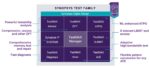
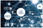
With this backdrop, TSMC introduced the 3Dblox™ Standard. This standard implements a language that provides a consistent way specify all requirements for a 2.5/3D design. It is an ambitious project that unifies all aspect of 2.5/3D design specification, as shown in the figure.
Thanks to TSMC’s extensive OIP ecosystem, all the key EDA providers support the 3Dblox language, making it possible to perform product design in a unified way, independent of a specific tool flow.
This capability ties it all together for the product designer. The Next Big Thing is now within reach, since TSMC redefines foundry to enable next-generation products.
Also Read:
TSMC Doubles Down on Semiconductor Packaging!
TSMC Clarified CAPEX and Revenue for 2023!
TSMC 2023 North America Technology Symposium Overview Part 3

