
Our laptops and desktop computers have billions of transistors in their application processor chips, yet I often don’t consider the reliability effects of aging that the transistors experience in the chips. At the recent Synopsys User Group (aka SNUG), there was a technical presentation on this topic from Srinivas Bodapati, an engineer at Intel.
Device Aging
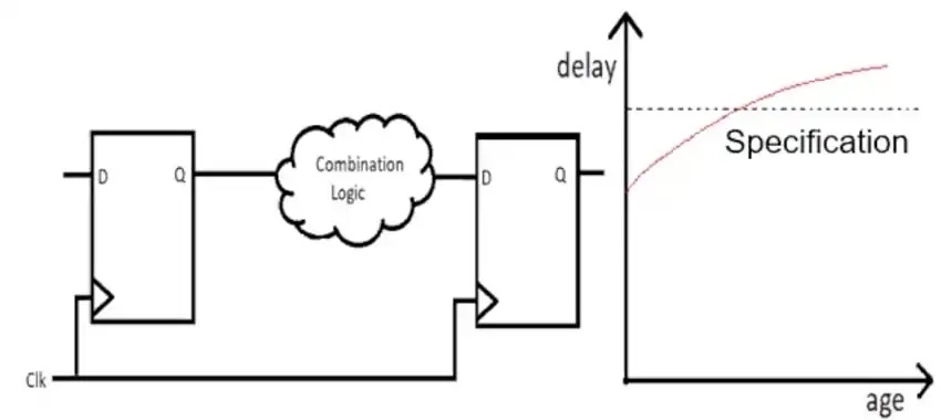
As transistors are switched on and off the drain currents can over time slowly decrease, this in turn changes path delays that make the chip speed slow down, and even fail to meet specifications. Device aging is now a first order problem when designing leading edge processor chips and GPUs. To manage power dissipation, many SoC design employ Dynamic Voltage Frequency Scaling (DVFS) techniques, yet the stress from running with a high VDD begins to impact circuit operation when in low VDD mode.

Device aging is dependent on workload, Voltage, Temperature and Frequency, and the two effects that cause transistor performance to shift over age are:
- Bias Temperature Instability (BTI)
- Hot Carriers Injection (HCI)
The device aging mechanisms for HCI and BTI are summarized in this table as a function of each factor:

At 14nm the main aging contribution was from BTI, but at 10nm it was from HCI effects. At the same time the End Of Life (EOL) drive currents increased by 1.65X, going from 14nm to 10nm.

Use Condition Problems
With DVFS circuits during the high VDD frequency mode there is stress to the transistors, which then impacts the circuit operation in low VDD mode. The delay of gates can become slower through aging, even to the point of getting out of specification, causing a timing failure.
During Static Timing Analysis (STA), the challenge is to model the workload dependency of aging, and consider that input slope plus output load impact aging. Consider an SoC example where there is a high performance core (PCore), an efficiency core (Ecore), fabric, and system IP blocks. These four types of IP have very different supply voltage ranges, and also temperatures. Trying to use the same static guard band for each IP block would be overly pessimistic for some scenarios, so using an existing aged library cannot really capture all of the various stress scenarios.

STA Aging Model Complexity
In the example below there’s a launch path, and a capture path, but each path has a unique switching activity which then changes their aging degradation to be different amounts. For each path the effects of both BTI and HCI also need to be taken into account, as aging degradation depends on each

Old and New Approaches
The older approach was to use STA with Aged Libraries and then have path simulation for derates. The drawbacks of the older approach are that DVFS usage is not accounted for, the BTI vs HCI effects are not separated, and it required handcrafted paths. The other challenge is the productivity bottleneck, as the STA and simulation are typically handled by different expert teams, modeling aging involves multiple cycles of identifying paths, running simulations, and analyzing results to come up with derates, which can then be used for modeling aging, however, these derates can often be pessimistic.
The new approach is an aging-aware STA methodology, which has automated workload dependency, simulates actual paths, takes into account BTI and HCI tradeoffs, works within a single simulation structure, and supports scalability of aging mission profiles without trading off for accuracy and enabling them to find the actual worst-case.
Aging-Aware STA Flow
The Synopsys tool for this aging-aware flow is called PrimeShield, and there are two components:
- Aging STA
- Aging-aware SPICE simulation
Intel used the aging-aware SPICE simulation component, where the circuit designer specifies a set of paths for simulation in Simlink. This enabled the specify and create stress conditions and simulates with HSPICE creating a degradation file that is used to generate playback with fresh conditions to measure the aging impact. Aging-aware Simlink enables easier stress conditions creation and automates the impact of aging at various other stress condition, based on initial inputs.

On the other hand aging-aware STA flow eases the methodology further by using aged libraries with mission profile information to calculate the impact of aging on the actual paths using the Synopsys PrimeTime’s PBA methodology. It also enables designers to configures the stress waveform by setting the cycle count, an activity factor, a signal probability, age time, and stress voltage ratio.
Results
Using the aging-aware flow they wanted to see the workload dependency of slack degradation, and the reference case is called slack2, where both the launch clock and capture clock have an activity factor of 0.2, shown in the table below:

Slack2 is the reference scenario, with equal activity factors for launch and capture clocks. The other three scenarios have a variety of activity factors for launch and capture clocks, and the yellow table shows how the slack degradation increases for each scenario, with scenario slack82 having the worst case slack degradation. These results depend on the effects of HCI and BTI.
Running and plotting many paths to compare normalized degraded slack versus normalized reference slack is shown in the next plot. The legend shows four types of results:
- Launch clock at 0.2, capture clock at 0.2 (l2c2)
- Launch clock at 0.8, capture clock at 0.8 (l8c8)
- Launch clock at 0.8, capture clock at 0.3 (l8c2)
- Launch clock at 0.2, capture clock at 0.8 (l2c8)

This helps designers identify worst case corners for each IP block in a path aging flow.
Conclusions
Running STA with aging effects is quite complex, especially when using DVFS design techniques, and aging depends on workloads to get accurate answers. Intel designers working with Synopsys tools and AEs have developed an aging-aware STA flow that uses PrimeShield, Simlink and HSPICE together for path simulations. Reliability issues are now first order, so having automation for aging analysis in a STA flow is a must have feature.
Related Blogs
- Delivering Systemic Innovation to Power the Era of SysMoore
- Synopsys Enhances Chips and Systems with New Silicon Lifecycle Management Platform
- Casting Light on OpenLight’s Open Silicon Photonics Platform
- DesignDash: ML-Driven Big Data Analytics Technology for Smarter SoC Design


Comments
There are no comments yet.
You must register or log in to view/post comments.