
At the 2022 SPIE Advanced Lithography Conference, ASML presented an update on EUV. I recently had a chance to go over the presentations with Mike Lercel of ASML. The following is a summary of our discussions.
0.33 NA
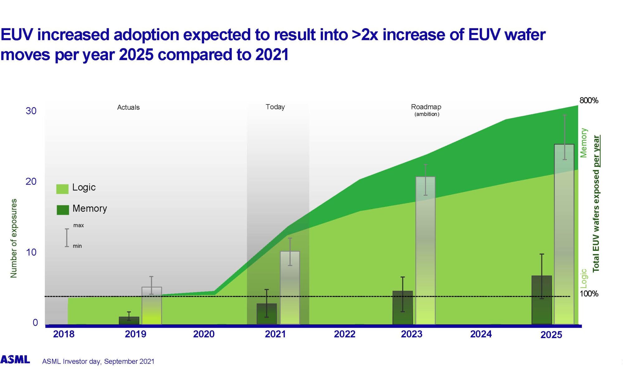
The 0.33 NA EUV systems are the production workhorse systems for leading edge lithography today. 0.33 NA systems are in high volume production for both logic and DRAM. Figure 1 illustrates the number of EUV layers for logic and DRAM (bars) and wafers exposed per year (area). Authors note, the 2021 values for logic are typical of foundry 5nm processes at 10+ EUV layers and 2023 logic would be in-line with foundry 3nm processes at ~20 layers, DRAM usages is currently ~5 layers. I asked mike about future DRAM exposures, he pointed out there are ~8 critical layers on a DRAM and eventually some of those layers could need multi-patterning bringing EUV exposure up to 10 per wafers.

Figure 1. EUV Adoption.
Through Q1 of 2022 ASML has shipped 136 EUV systems and ~70 million wafers have been exposed, see figure 2.

Figure 2. Number of EUV Wafers Exposed.
System availability continues to improve, it is at a little less than 90% today. The new NXE:3600D is better than the NXE:3400C and provide ~93% availability. EUV system availability is getting close to DUV system levels (~95%).

Figure 3. Availability.
NXE:3600D systems can produce 160 wafers per hour (wph) at 30mJ/cm2, 18% better than the NXE:3400C. The NXE:3800E systems in development will provide >195 wph at 30mJ/cm2 initially, and 220 wph with throughput upgrades. The NXE:3600E will have incremental optical improvements in aberration, overlay and throughput.

Figure 4. Throughput Improvements.
Matched machine overlay for the NXE:3400C was 1.5nm and is 1.1nm for the NXE:3600D. The NXE:3600D uses the same new 12 wavelength alignment system as the newest DUV systems with just a few material differences due to vacuum use.
The ASML roadmap includes the NXE:4000F with >220wph around 2025, see figure 5.

Figure 5. System Roadmap.
Pellicles now achieve greater than 90% transmission and manufacturing has been transferred to Mitsui. I run into people from time to time who think Pellicles are a future EUV item, but Pellicles have been in production use on select layers for over a year.

Figure 6. Pellicle Performance.
Finally for the 0.33 NA system ASML is working on reducing the energy required for each exposure by increasing throughput and decreasing total energy.

Figure 7. Energy Per Exposure.
We discussed the ultimate resolution limits for 0.33 NA systems, in theory 0.33 NA can produce 26nm in a single exposure, currently Imec is working on 28nm single exposure, but it isn’t in production yet.
0.55 NA (High NA)
As described in the previous section 0.33 NA EUV is in high volume production. Leading edge foundry processes have now reached the 3nm “node” and double patterning with 0.33 NA EUV is becoming necessary. By raising the NA from 0.33 to 0.55 double patterned layers can be replaced with single exposures.
Figure 8 illustrates how DUV layers counts grew driven by process complexity and multipatterning until 0.33 NA EUV took over eliminating a lot of multipatterning. As 0.33 NA EUV multipatterning use grows 0.55 NA EUV can eliminate some multipatterning reducing layer counts again.

Figure 8. Mask Count Trends.
High-NA provides a better image log slope, stochastic defects are 3D and high-NA helps with defect reduction. ASML is working on attenuated phase shift masks for EUV to improve contrast and depth of field. They will be implemented for 0.33 NA first and then 0.55 NA later.
ASML’s roadmap has the first High NA system (EXE:5000) being installed in a lab at the ASML factory run jointly with Imec in 2023 for initial evaluation. EXE:5000 systems should be delivered to customers in 2024 and the production EXE:5200 system should be delivered to customers for production use around 2025, see figure 9.

Figure 9. High-NA System Roadmap.
The optics for High-NA are significantly larger than for 0.33 NA and require a unique design approach. 0.55 NA systems will have an anamorphic lens system with a 4x reduction ratio in one direction (the same as 0.33 NA) and an 8x reduction ratio in the orthogonal direction. Due to the size of the reticle and the 8x reduction, the printable field size is cut in half to 16.5nm in the scan direction, see figure 10.

Figure 10. Anamorphic Lens System.
Simulations show no direction differences between a half-field and full field exposure. Half-field exposures can be aligned to full field exposures so that existing DUV and 0.33 NA EUV systems can be used in a mix and match strategy with 0.55 NA systems. If necessary for large die, 0.55 NA half-field exposures can stitched together, possibly with a small stitch boundary for global connections.
Using research tools at The Center for X-Ray Optics at Berkely and Paul Scherrer Institut, ASML has been able to demonstrate High-NA EUV resolution down to 8, see figure 11.

Figure 11. 8nm Line/Spaces.
The 0.55 NA system design is broken up into 4 independently testable sub systems (see figure 12) and assembly of the first exposure tool to go into the ASML/Imec lab in 2023 has begun (see figure 13).

Figure 12. High-NA Sub Systems.

Figure 13. 0.55 NA System Integration.
ASML continues to work on increasing source power and has recently demonstrated >500 watts in research. Historically it has taken ~2 years for research developments to reach production. Figure 14 illustrates source power over time.

Figure 14. Source Power Trends.
0.7 NA
In a recent article Tom Dillinger discussed an interview with Mark Phillips of Intel and Mark mentioned 0.7 NA as a successor to 0.55 NA. I was surprised by this, I thought ASML had ruled out developing anything after 0.55 NA due to the high investments ASML has had to make on EUV. Mike said ASML hasn’t ruled out a 0.7 or greater NA system, they are looking at it. He said they have ruled out shorter wavelengths than the current 13.5nm (authors note, at one time there was some discussion of a shorter wavelength system 6.xnm). They do want any new system to be air shippable which limits how much bigger the system can be than the 0.55 NA systems.
Conclusion
0.33 NA EUV systems are now production work horse systems with continuously improving availability and throughput. 0.55 NA systems are expected to enter production in 2025 with higher resolution enabling process simplification. Beyond 0.55 NA ASML is looking at even higher NA systems. EUV is well positioned to continue to drive lithography resolution for the next decade.
Also Read:
Obscuration-Induced Pitch Incompatibilities in High-NA EUV Lithography
The Electron Spread Function in EUV Lithography
Double Diffraction in EUV Masks: Seeing Through The Illusion of Symmetry
Share this post via:


Comments
5 Replies to “ASML EUV Update at SPIE”
You must register or log in to view/post comments.