

If you’ve designed a chip with analog content (and who hasn’t), you know Analog Bits. Along the way, you likely met Mahesh. If you are a lover of fine wines, you probably know Mahesh quite well. More on that later. I got the opportunity to speak with him recently about what he’s been up to, both now and over the past few years. It’s a story about a love for technology and a love for wine. If you believe that wine is an art form, then the statement “life imitates art” is very relevant to what follows. Read on to learn about the incredible journey of Analog Bits through the eyes of Mahesh Tirupattur.
Wine, and Life Imitating Art
Just like in the high-tech world of Silicon Valley, there are many M&A transactions occurring in Napa Valley and beyond. Private equity firms are acquiring and consolidating many of the large wineries we’ve come to know and love over the years. While the details of these transactions are often not public, I do know a few facts about some of the larger ones, thanks to my love for wine and the connections I’ve made along the way.
The model for several of these deals is quite unique. A private equity firm will acquire a controlling interest in a winery and then essentially do nothing, allowing the original creativity to flow unhindered. The message to the owners is simple – we love your wine and the brand you’ve built. Please continue to do what you do regarding making your product. We’ll worry about the operational details. And when you’re ready to step down, just call us and we’ll be ready to take over. Until then, keep focused on your passion.
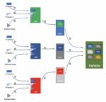
This laissez faire acquisition strategy from the wine industry has found its way to other transactions as well. Case in point being the acquisition of Analog Bits by SEMIFIVE that occurred about a year and half ago. As covered on SemiWiki here, there is a variety of business models and foundry relationships that comprise the combination of these two companies. SEMIFIVE is the pioneer of platform-based SoC design, working with customers to implement innovative ideas into custom silicon in the most efficient way. The company has a close relationship with Samsung Foundry. Analog Bits is the leader in developing and delivering low-power integrated clocking, sensors and interconnect IP that are pervasive in virtually all of today’s semiconductors. The company has not only developed IP on the Samsung process, but it also has a close and growing relationship with TSMC.
One approach (and a common one) would be to combine the operations of both companies into one model with one set of relationships. That would cause a significant ripple effect in one or both of these company’s businesses, and not a good ripple effect. Rather than do that, SEMIFIVE took a page out of the winery acquisition playbook being used in Napa Valley and elsewhere.
Analog Bits continues to operate as an independent entity, but now as part of a larger enterprise. The company continues to do the things it loves to do, providing critical enabling IP that its customers need. Dan Nenni summarized it well in the SemiWiki post:
To me this acquisition is another 1+1=3. SEMIFIVE gets a strong IP base in North America plus foundry and customer relationships that have been silicon proven for 20+ years. Analog Bits gets the ability to scale rapidly and increase the depth and breadth of their IP offering.
I mentioned a connection between Mahesh and wine earlier. It turns out he is quite an accomplished Sommelier as well as a technologist, completing three of the four levels that pave the way to Master Sommelier. While there is still more road ahead for Mahesh to achieve this ultimate title, his progress in the face of also building a very successful IP business is noteworthy. There are 269 Master Sommeliers in the world today. This is truly a rare achievement. Mahesh has also become an expert in the making of Sake, which he claims is far more complex and nuanced than wine.
Perhaps this is the topic of a future blog post or podcast.
The Road Ahead
During my discussions with Mahesh, it was quite clear that he was happy with the outcome of the acquisition. The ability to continue to operate independently, continuing to do what he loves with the backing of a larger enterprise feels good. I can imagine the winemakers that were part of the Napa Valley acquisitions saying the same thing.
He talked about the great position Analog Bits enjoys in the development of purpose-built IP blocks for various high-growth markets. The track record and customer-focused nature of the company make this a great match. Mahesh talked about many new market opportunities. One interesting one is power management and spike detection. With so many cores and power domains in advanced designs, often fueled by AI, power spikes have become a very real liability. Analog Bits is developing on-chip IP to sense and manage these events.
Overall, Analog Bits is becoming more “sticky” for advanced designs thanks to their broad catalog and excellent track record. According to Mahesh, the future is bright and a larger operation at Analog Bits seems likely. And that’s just part of the incredible journey of Analog Bits through the eyes of Mahesh Tirupattur.


