Synopsys has just announced that it has expanded its ARC processor portfolio to include a family of RISC-V processors. These will be branded under the ARC name as ARC-V and are expected to become available in 2024. This is a significant announcement which I attempt to unpack briefly below.
Why add RISC-V to the portfolio and why now?
I talked to Rich Wawrzyniak, principal analyst at the SHD Group to get a sense of the opportunity. He is working on a market assessment in collaboration with RISC-V International (see above). This unsurprisingly shows very healthy growth across all major business segments, maybe 30%+ CAGR up through 2030. Business growth opportunities like that are not thick on the ground so I can see the appeal to Synopsys.
Rich also points out that the design opportunity is not a one-size-fits-all per SoC. Heterogeneity within an SoC now extends not only to processor types (CPU, DSP, AI, etc) but also to architectures (Arm versus RISC-V for example). I imagine multi-die systems will reinforce this trend. In a different class of applications, I have seen interest in combining a RISC-V controller with a DSP and possibly a dedicated AI engine for ultra-low power/tight margin applications. Given ARC strength in DSP processors this enhanced ARC portfolio would be an obvious fit.
The initial product offering
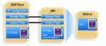
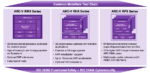
There are three families in the announcement. The ARC-V RMX Series is designed for ultra-low power applications. Think of motor controllers, BLE control, SD cards and hearables. Very much targeted to deep embedded applications. The ARC-V RHX Series is aimed at higher performance real-time applications, such as safety managers in a car, robotics, medical devices, and computational storage. This series offers virtualization support, for example for multi-core clusters in a car which must handle a variety of changing workloads. The ARC-V RPX Series is designed for host processors, intended for applications such as avionics, medical imaging, car zonal controllers, storage area networks.
Naturally Synopsys will extend their functional safety/security experience and IP expertise to all these products. They will also provide extensibility options as appropriate to target markets, such as DSP extensions for ARC-V RMX Series and RVV extensions for RHX. The Metaware toolchain, already well established with other ARC cores is being extended to support ARC-V cores providing compiler, debugger, and ISA simulator development tools. Synopsys are also working on extending their software ecosystem beyond an existing rich set of partners supporting ARC IPs to fold in more of the complementary RISC-V group.
Rich Collins (Director of Product Management, Solutions Group, Synopsys) tells me Synopsys is not looking at server or mobile applications today, though as an active member (and board member) of RISC-V international they will continue to track evolving profiles and no doubt add to this family over time.
What does this mean for the processor cores market?
Synopsys is by far the dominant supplier of hardware (and related software) IP in the market and have proven expertise and systems to develop, support and deliver IP to a wide customer base. They have close relationships with foundries and standard bodies, they have all their own silicon lifecycle development tools and processes in house, from prototyping to implementation, verification and tape-out, now extending to multi-die systems. Together with software development tools. All this is very good news for system builders looking for a strong and long-term RISC-V IP supplier. Also good news for Synopsys who I have no doubt will make a success of this business.
What follows beyond this point is solely my opinion. The RISC-V ISA standard remains open, and I don’t see system builders with their own RISC-V implementations thinking they need to switch because Synopsys now has an offering. What is less clear is what happens to the rest of the RISC-V core and EDA market. A small company today will need a pretty strong, differentiated value prop to stand against Synopsys. In time I am sure newer and more radical propositions will appear (this is tech after all).
Arm versus Synopsys RISC-V is a different story. Arm is also very experienced in developing, delivering, and supporting their IP. They have deep foundry, standards committees, and EDA relationships. And their singular focus (mostly) on processors means they can invest heavily in that area. As an example, they are thought to invest $100M/year in verification alone. That’s a big number backed by a long learning curve of working with a worldwide customer base across a huge number of applications.
Which doesn’t mean they couldn’t be displaced but in high value markets I expect those battles would be very hard fought. I think a more likely outcome is a duopoly between Arm and Synopsys ARC-V. They both need each other, Arm for the design lifecycle support infrastructure and Synopsys for the Arm loyalists. Around the fringes will be system builders happy to build and maintain their own cores and startups with new creative ideas to do something really different around RISC-V. Not so much “me too” cores or infrastructure. My two cents.
Big news. You can read the press release HERE.