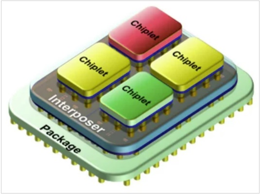
The first Chiplet specific conference is coming up which is a milestone in itself. As we know the only thing new about chiplets is the name but when there is a dedicated conference to such a specific thing you know it has officially “arrived”. There is even a cool new tagline: Chiplets make huge chips happen!
“The First Annual Chiplet Summit is the show chip designers can’t miss if they want to stay competitive. They’ll get the scoop on ways to make their chiplets run faster, scale better, use less power, and be more flexible. This unique event gives attendees a place to network with peers, ask questions of the experts, and talk to vendors offering a wide variety of products and services.”
The Chiplet Summit (January 24-26th) is brought to us by the folks who do the very successful Flash Memory Summit. There are three full days of conference with a pre conference day on Tuesday and regular conference days on Wednesday and Thursday. Given live conferences of late are back to pre-pandemic levels I would expect a full house. Quite a few companies that work with SemiWiki will be presenting so I of course will be there too. If you are there look me up, it would be a pleasure to meet you.
There is a great keynote line up with some very familiar faces. One of the more notable ones is the Daniel Armburst co-founder of Silicon Catalyst who is speaking on “How Chiplets Can Help You Profit from Chips for America”.
Abstract:
The semiconductor industry has evolved over six decades from its origin in startups, venture capital, and vertically integrated companies to a robustly growing, horizontally integrated and concentrated supply chain. Chiplets are one of the major trends that will shape the future winners and losers and resulting industry structure. Chiplets will also be essential for accelerating startup innovation and addressing designer productivity.
While die aggregation has become a reality for many important companies, replicating that success has yet to be achieved for packaging aggregation of commonly available chiplets. Several critical business model challenges and ecosystem developments are required to get to a vibrant standards-based chiplets world.
With the passage of the $52B CHIPS Act in the U.S. and similar initiatives elsewhere in the world, there should be ample opportunities to accelerate the timelines and benefits for industry, government and academic stakeholders.
So, back to the chiplet war, to me chiplets are all about design enablement: getting designs to wafer faster, cheaper, and with less risk of failure (yield). And who does that really benefit the most? TSMC of course. In fact, design/wafer enablement is what the TSMC OIP is all about.
In order for chiplets to work there must be an ecosystem that documents the provenance of the chiplet and that is what TSMC already does for EDA tools, commercial IP, and other critical parts of design enablement. Nobody is better at ecosystem building than TSMC and it really is like a snowball rolling down Mount Everest.
The semiconductor IP industry will also win big. Chiplets brings royalty IP licensing back into focus. Getting paid per chip really is the IP holy grail and something Wall Street greatly respects. I have personal experience in collecting IP royalty revenue from foundries which was quite a challenge. Arm perfected this model as did the former Artisan Components back in the 1990s. Arm then purchased Artisan for an amazing $900M and the IP royalty model was a key component in the acquisition.
But as I said, getting a royalty agreement is hard enough but collecting those royalties was even harder. With chiplets you will be selling die so it is more of a chip sale than a royalty play. This should simplify the chiplet IP monetization process dramatically and greatly appeal to Wall Street, VCs, and other financial backers of the semiconductor ecosystem, absolutely.
Also Read:
Chiplets UCIe Require Verification
Synopsys Crosses $5 Billion Milestone!
Share this post via:


Solving the EDA tool fragmentation crisis